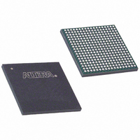
EP3C25F324I7 Altera, EP3C25F324I7 Datasheet - Page 55

EP3C25F324I7
Manufacturer Part Number
EP3C25F324I7
Description
IC CYCLONE III FPGA 25K 324 FBGA
Manufacturer
Altera
Series
Cyclone® IIIr
Datasheets
1.EP3C5F256C8N.pdf
(5 pages)
2.EP3C5F256C8N.pdf
(34 pages)
3.EP3C5F256C8N.pdf
(66 pages)
4.EP3C5F256C8N.pdf
(14 pages)
5.EP3C5F256C8N.pdf
(76 pages)
6.EP3C25F324I7.pdf
(274 pages)
Specifications of EP3C25F324I7
Number Of Logic Elements/cells
24624
Number Of Labs/clbs
1539
Total Ram Bits
608256
Number Of I /o
215
Voltage - Supply
1.15 V ~ 1.25 V
Mounting Type
Surface Mount
Operating Temperature
-40°C ~ 100°C
Package / Case
324-FBGA
Family Name
Cyclone III
Number Of Logic Blocks/elements
24624
# I/os (max)
215
Frequency (max)
437.5MHz
Process Technology
65nm
Operating Supply Voltage (typ)
1.2V
Logic Cells
24624
Ram Bits
608256
Operating Supply Voltage (min)
1.15V
Operating Supply Voltage (max)
1.25V
Operating Temp Range
-40C to 100C
Operating Temperature Classification
Industrial
Mounting
Surface Mount
Pin Count
324
Package Type
FBGA
For Use With
544-2370 - KIT STARTER CYCLONE III EP3C25
Lead Free Status / RoHS Status
Contains lead / RoHS non-compliant
Number Of Gates
-
Lead Free Status / Rohs Status
Not Compliant
Available stocks
Company
Part Number
Manufacturer
Quantity
Price
Company:
Part Number:
EP3C25F324I7N
Manufacturer:
ALTERA32
Quantity:
181
Chapter 3: Memory Blocks in the Cyclone III Device Family
Chapter Revision History
Power-Up Conditions and Memory Initialization
Power Management
Chapter Revision History
Table 3–6. Chapter Revision History
© December 2009
December 2009
July 2009
June 2009
October 2008
May 2008
July 2007
March 2007
Date
f
Altera Corporation
The M9K memory block outputs of the Cyclone III device family power up to zero
(cleared) regardless of whether the output registers are used or bypassed. All M9K
memory blocks support initialization using a .mif. You can create .mifs in the
Quartus II software and specify their use using the RAM MegaWizard Plug-In
Manager when instantiating memory in your design. Even if memory is
pre-initialized (for example, using a .mif), it still powers up with its outputs cleared.
Only the subsequent read after power up outputs the pre-initialized values.
For more information about .mifs, refer to the
Quartus II
The M9K memory block clock enables of the Cyclone III device family allow you to
control clocking of each M9K memory block to reduce AC power consumption. Use
the rden signal to ensure that read operations only occur when necessary. If your
design does not require read-during-write, reduce power consumption by deasserting
the rden signal during write operations, or any period when there are no memory
operations. The Quartus II software automatically powers down any unused M9K
memory blocks to save static power.
Table 3–6
Version
2.2
2.1
2.0
1.3
1.2
1.1
1.0
lists the revision history for this chapter.
Handbook.
Minor changes to the text.
Made minor correction to the part number.
Updated to include Cyclone III LS information
■
■
■
■
■
■
■
■
Updated chapter to new template.
■
■
Added chapter TOC and “Referenced Documents” section.
Initial release.
Updated chapter part number.
Updated “Introduction” on page 3–1.
Updated “Overview” on page 3–1.
Updated Table 3–1 on page 3–2.
Updated “Control Signals” on page 3–3.
Updated “Memory Modes” on page 3–8.
Updated “Simple Dual-Port Mode” on page 3–10.
Updated “Read or Write Clock Mode” on page 3–16.
Revised the maximum performance of the M9K blocks to 315 MHz in
“Introduction” and “Overview” sections, and in Table 3-1.
Updated “Address Clock Enable Support” section.
Changes Made
RAM Megafunction User Guide
Cyclone III Device Handbook, Volume 1
and the
3–19


