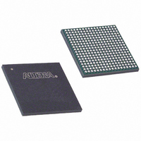
EP3C25F324I7 Altera, EP3C25F324I7 Datasheet - Page 90

EP3C25F324I7
Manufacturer Part Number
EP3C25F324I7
Description
IC CYCLONE III FPGA 25K 324 FBGA
Manufacturer
Altera
Series
Cyclone® IIIr
Datasheets
1.EP3C5F256C8N.pdf
(5 pages)
2.EP3C5F256C8N.pdf
(34 pages)
3.EP3C5F256C8N.pdf
(66 pages)
4.EP3C5F256C8N.pdf
(14 pages)
5.EP3C5F256C8N.pdf
(76 pages)
6.EP3C25F324I7.pdf
(274 pages)
Specifications of EP3C25F324I7
Number Of Logic Elements/cells
24624
Number Of Labs/clbs
1539
Total Ram Bits
608256
Number Of I /o
215
Voltage - Supply
1.15 V ~ 1.25 V
Mounting Type
Surface Mount
Operating Temperature
-40°C ~ 100°C
Package / Case
324-FBGA
Family Name
Cyclone III
Number Of Logic Blocks/elements
24624
# I/os (max)
215
Frequency (max)
437.5MHz
Process Technology
65nm
Operating Supply Voltage (typ)
1.2V
Logic Cells
24624
Ram Bits
608256
Operating Supply Voltage (min)
1.15V
Operating Supply Voltage (max)
1.25V
Operating Temp Range
-40C to 100C
Operating Temperature Classification
Industrial
Mounting
Surface Mount
Pin Count
324
Package Type
FBGA
For Use With
544-2370 - KIT STARTER CYCLONE III EP3C25
Lead Free Status / RoHS Status
Contains lead / RoHS non-compliant
Number Of Gates
-
Lead Free Status / Rohs Status
Not Compliant
Available stocks
Company
Part Number
Manufacturer
Quantity
Price
Company:
Part Number:
EP3C25F324I7N
Manufacturer:
ALTERA32
Quantity:
181
5–26
Figure 5–21. PLL Reconfiguration Scan Chain
Cyclone III Device Handbook, Volume 1
configupdate
scandataout
scanclkena
scandone
scandata
scanclk
areset
1
1
The counter settings are updated synchronously to the clock frequency of the
individual counters. Therefore, not all counters update simultaneously.
To reconfigure the PLL counters, perform the following steps:
1. The scanclkena signal is asserted at least one scanclk cycle prior to shifting in
2. Serial data (scandata) is shifted into the scan chain on the second rising edge of
3. After all 144 bits have been scanned into the scan chain, the scanclkena signal is
4. The configupdate signal is asserted for one scanclk cycle to update the PLL
5. The scandone signal goes high indicating that the PLL is being reconfigured. A
6. Reset the PLL using the areset signal if you make any changes to the M, N,
7. You can repeat steps
Figure 5–21
When reconfiguring the counter clock frequency, the corresponding counter phase
shift settings cannot be reconfigured using the same interface. You can reconfigure
phase shifts in real time using the dynamic phase shift reconfiguration interface. If
you reconfigure the counter frequency, but wish to keep the same non-zero phase
shift setting (for example, 90°) on the clock output, you must reconfigure the phase
shift after reconfiguring the counter clock frequency.
Dn_old
the first bit of scandata (Dn).
scanclk.
deasserted to prevent inadvertent shifting of bits in the scan chain.
counters with the contents of the scan chain.
falling edge indicates that the PLL counters have been updated with new settings.
post-scale output C counters, or the I
Dn
shows a functional simulation of the PLL reconfiguration feature.
1
through
Chapter 5: Clock Networks and PLLs in the Cyclone III Device Family
5
to reconfigure the PLL any number of times.
CP
, R, C settings.
D0_old
LSB
D0
© December 2009 Altera Corporation
Dn
PLL Reconfiguration


