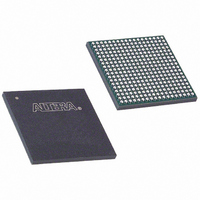
EP3C25F324I7 Altera, EP3C25F324I7 Datasheet - Page 76

EP3C25F324I7
Manufacturer Part Number
EP3C25F324I7
Description
IC CYCLONE III FPGA 25K 324 FBGA
Manufacturer
Altera
Series
Cyclone® IIIr
Datasheets
1.EP3C5F256C8N.pdf
(5 pages)
2.EP3C5F256C8N.pdf
(34 pages)
3.EP3C5F256C8N.pdf
(66 pages)
4.EP3C5F256C8N.pdf
(14 pages)
5.EP3C5F256C8N.pdf
(76 pages)
6.EP3C25F324I7.pdf
(274 pages)
Specifications of EP3C25F324I7
Number Of Logic Elements/cells
24624
Number Of Labs/clbs
1539
Total Ram Bits
608256
Number Of I /o
215
Voltage - Supply
1.15 V ~ 1.25 V
Mounting Type
Surface Mount
Operating Temperature
-40°C ~ 100°C
Package / Case
324-FBGA
Family Name
Cyclone III
Number Of Logic Blocks/elements
24624
# I/os (max)
215
Frequency (max)
437.5MHz
Process Technology
65nm
Operating Supply Voltage (typ)
1.2V
Logic Cells
24624
Ram Bits
608256
Operating Supply Voltage (min)
1.15V
Operating Supply Voltage (max)
1.25V
Operating Temp Range
-40C to 100C
Operating Temperature Classification
Industrial
Mounting
Surface Mount
Pin Count
324
Package Type
FBGA
For Use With
544-2370 - KIT STARTER CYCLONE III EP3C25
Lead Free Status / RoHS Status
Contains lead / RoHS non-compliant
Number Of Gates
-
Lead Free Status / Rohs Status
Not Compliant
Available stocks
Company
Part Number
Manufacturer
Quantity
Price
Company:
Part Number:
EP3C25F324I7N
Manufacturer:
ALTERA32
Quantity:
181
5–12
Clock Feedback Modes
Source-Synchronous Mode
Cyclone III Device Handbook, Volume 1
1
Cyclone III device family PLLs support up to four different clock feedback modes.
Each mode allows clock multiplication and division, phase shifting, and
programmable duty cycle.
Input and output delays are fully compensated by the PLL only when you are using
the dedicated clock input pins associated with a given PLL as the clock sources. For
example, when using PLL1 in normal mode, the clock delays from the input pin to the
PLL and the PLL clock output-to-destination register are fully compensated, provided
that the clock input pin is one of the following four pins:
■
■
■
■
When driving the PLL using the GCLK network, the input and output delays may not
be fully compensated in the Quartus II software.
If the data and clock arrive at the same time at the input pins, the phase relationship
between the data and clock remains the same at the data and clock ports of any I/O
element input register.
Figure 5–8
mode for source-synchronous data transfers. Data and clock signals at the I/O
element experience similar buffer delays as long as the same I/O standard is used.
Figure 5–8. Phase Relationship Between Data and Clock in Source-Synchronous Mode
Source-synchronous mode compensates for delay of the clock network used,
including any difference in the delay between the following two paths:
■
■
CLK0
CLK1
CLK2
CLK3
Data pin to I/O element register input
Clock input pin to the PLL phase-frequency detector (PFD) input
shows an example waveform of the data and clock in this mode. Use this
clock at input pin
Clock at register
Data at register
PLL reference
Data pin
Chapter 5: Clock Networks and PLLs in the Cyclone III Device Family
© December 2009 Altera Corporation
Clock Feedback Modes


