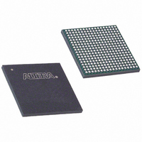
EP3C25F324I7 Altera, EP3C25F324I7 Datasheet - Page 186

EP3C25F324I7
Manufacturer Part Number
EP3C25F324I7
Description
IC CYCLONE III FPGA 25K 324 FBGA
Manufacturer
Altera
Series
Cyclone® IIIr
Datasheets
1.EP3C5F256C8N.pdf
(5 pages)
2.EP3C5F256C8N.pdf
(34 pages)
3.EP3C5F256C8N.pdf
(66 pages)
4.EP3C5F256C8N.pdf
(14 pages)
5.EP3C5F256C8N.pdf
(76 pages)
6.EP3C25F324I7.pdf
(274 pages)
Specifications of EP3C25F324I7
Number Of Logic Elements/cells
24624
Number Of Labs/clbs
1539
Total Ram Bits
608256
Number Of I /o
215
Voltage - Supply
1.15 V ~ 1.25 V
Mounting Type
Surface Mount
Operating Temperature
-40°C ~ 100°C
Package / Case
324-FBGA
Family Name
Cyclone III
Number Of Logic Blocks/elements
24624
# I/os (max)
215
Frequency (max)
437.5MHz
Process Technology
65nm
Operating Supply Voltage (typ)
1.2V
Logic Cells
24624
Ram Bits
608256
Operating Supply Voltage (min)
1.15V
Operating Supply Voltage (max)
1.25V
Operating Temp Range
-40C to 100C
Operating Temperature Classification
Industrial
Mounting
Surface Mount
Pin Count
324
Package Type
FBGA
For Use With
544-2370 - KIT STARTER CYCLONE III EP3C25
Lead Free Status / RoHS Status
Contains lead / RoHS non-compliant
Number Of Gates
-
Lead Free Status / Rohs Status
Not Compliant
Available stocks
Company
Part Number
Manufacturer
Quantity
Price
Company:
Part Number:
EP3C25F324I7N
Manufacturer:
ALTERA32
Quantity:
181
9–26
Figure 9–8. Single-Device AP Configuration Using Numonyx P30 and P33 Flash Memory
Notes to
(1) Connect the pull-up resistors to the V
(2) The nCEO pin is left unconnected or used as a user I/O pin when it does not feed the nCE pin of another device.
(3) The MSEL pin settings vary for different configuration voltage standards and POR time. To connect MSEL[3..0], refer to
(4) The AP configuration ignores the WAIT signal during configuration mode. However, if you are accessing flash during user mode with user logic,
Cyclone III Device Handbook, Volume 1
page
you can optionally use a normal I/O to monitor the WAIT signal from the Numonyx P30 or P33 flash.
Figure
9–11. Connect the MSEL pins directly to V
9–8:
1
1
1
Numonyx P30/P33 Flash
The interface for the Numonyx P30 flash memory and P33 flash memory connects to
Cyclone III device pins, as shown in
In a single-device AP configuration, the maximum board loading and board trace
length between the supported parallel flash and Cyclone III devices must follow the
recommendations listed in
If you use the AP configuration scheme for Cyclone III devices, the V
1, 6, 7, and 8 must be 3.3, 3.0, 2.5, or 1.8 V. Altera does not recommend using the level
shifter between the Numonyx P30/P33 flash and the Cyclone III device in the AP
configuration scheme.
There are no series resistors required in the AP configuration mode for Cyclone III
devices when using the Numonyx flash at 2.5-, 3.0-, and 3.3-V I/O standard. The
output buffer of the Numonyx P30 IBIS model does not overshoot above 4.1 V. Thus,
series resistors are not required for the 2.5-, 3.0-, and 3.3-V AP configuration option.
However, if there are any other devices sharing the same flash I/Os with Cyclone III
devices, all shared pins are still subject to the 4.1-V limit and may require series
resistors.
Chapter 9: Configuration, Design Security, and Remote System Upgrades in the Cyclone III Device Family
DQ[15:0]
CCIO
A[24:1]
RST#
ADV#
WAIT
WE#
CLK
CE#
OE#
supply of the bank in which the pin resides.
CCA
or GND.
GND
Table 9–12 on page
10k
nCE
DCLK
nRESET
FLASH_nCE
nOE
nAVD
nWE
I/O (4)
DATA[15..0]
PADD[23..0]
V CCIO (1)
Figure
Cyclone III Device
10k
V CCIO (1) V CCIO (1)
9–8.
9–30.
10k
MSEL[3..0]
nCEO
© December 2009 Altera Corporation
N.C. (2)
(3)
CCIO
Configuration Features
Table 9–7 on
of I/O banks


