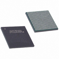
EP3C25F324I7 Altera, EP3C25F324I7 Datasheet - Page 157

EP3C25F324I7
Manufacturer Part Number
EP3C25F324I7
Description
IC CYCLONE III FPGA 25K 324 FBGA
Manufacturer
Altera
Series
Cyclone® IIIr
Datasheets
1.EP3C5F256C8N.pdf
(5 pages)
2.EP3C5F256C8N.pdf
(34 pages)
3.EP3C5F256C8N.pdf
(66 pages)
4.EP3C5F256C8N.pdf
(14 pages)
5.EP3C5F256C8N.pdf
(76 pages)
6.EP3C25F324I7.pdf
(274 pages)
Specifications of EP3C25F324I7
Number Of Logic Elements/cells
24624
Number Of Labs/clbs
1539
Total Ram Bits
608256
Number Of I /o
215
Voltage - Supply
1.15 V ~ 1.25 V
Mounting Type
Surface Mount
Operating Temperature
-40°C ~ 100°C
Package / Case
324-FBGA
Family Name
Cyclone III
Number Of Logic Blocks/elements
24624
# I/os (max)
215
Frequency (max)
437.5MHz
Process Technology
65nm
Operating Supply Voltage (typ)
1.2V
Logic Cells
24624
Ram Bits
608256
Operating Supply Voltage (min)
1.15V
Operating Supply Voltage (max)
1.25V
Operating Temp Range
-40C to 100C
Operating Temperature Classification
Industrial
Mounting
Surface Mount
Pin Count
324
Package Type
FBGA
For Use With
544-2370 - KIT STARTER CYCLONE III EP3C25
Lead Free Status / RoHS Status
Contains lead / RoHS non-compliant
Number Of Gates
-
Lead Free Status / Rohs Status
Not Compliant
Available stocks
Company
Part Number
Manufacturer
Quantity
Price
Company:
Part Number:
EP3C25F324I7N
Manufacturer:
ALTERA32
Quantity:
181
Chapter 8: External Memory Interfaces in the Cyclone III Device Family
Cyclone III Device Family Memory Interfaces Features
Figure 8–6. Extending the OE Disable by Half a Clock Cycle for a Write Transaction
Note to
(1) The waveform reflects the software simulation result. The OE signal is an active low on the device. However, the Quartus II software implements
OCT
PLL
© January 2010 Altera Corporation
the signal as an active high and automatically adds an inverter before the A
Figure
8–6:
f
f
1
from System Clock)
(outclock for DQS)
-90 phase shifted
(from logic array)
(from logic array)
(from logic array)
(from logic array)
(outclock for DQ,
Figure 8–6
high-impedance state by half a clock cycle during a write operation.
o
Cyclone III device family supports calibrated on-chip series termination (R
both vertical and horizontal I/O banks. To use the calibrated OCT, you must use the
RUP and RDN pins for each R
each OCT calibration block to calibrate one type of termination with the same V
that given side.
For more information about Cyclone III device family OCT calibration block, refer to
the
When interfacing with external memory, the PLL is used to generate the memory
system clock, the write clock, the capture clock and the logic-core clock. The system
clock generates the DQS write signals, commands, and addresses. The write-clock is
shifted by -90° from the system clock and generates the DQ signals during writes. You
can use the PLL reconfiguration feature to calibrate the read-capture phase shift to
balance the setup and hold margins.
The PLL is instantiated in the ALTMEMPHY megafunction. All outputs of the PLL are
used when the ALTMEMPHY megafunction is instantiated to interface with external
memories.
For more information about the usage of PLL outputs by the ALTMEMPHY
megafunction, refer to
System clock
OE for DQS
Write Clock
OE for DQ
datain_h
datain_I
Cyclone III Device I/O Features
DQS
DQ
shows how the second output enable register extends the DQS
90
o
Literature: External Memory
a Clock
by Half
Delay
Cycle
S
OCT control block (one for each side). You can use
chapter.
Preamble
OE
register D input.
D1
D0
D0
D1
Interfaces.
D3
D2
D2
(Note 1)
Cyclone III Device Handbook, Volume 1
D3
Postamble
S
OCT) in
CCIO
8–13
for


