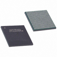
EP3C25F324I7 Altera, EP3C25F324I7 Datasheet - Page 270

EP3C25F324I7
Manufacturer Part Number
EP3C25F324I7
Description
IC CYCLONE III FPGA 25K 324 FBGA
Manufacturer
Altera
Series
Cyclone® IIIr
Datasheets
1.EP3C5F256C8N.pdf
(5 pages)
2.EP3C5F256C8N.pdf
(34 pages)
3.EP3C5F256C8N.pdf
(66 pages)
4.EP3C5F256C8N.pdf
(14 pages)
5.EP3C5F256C8N.pdf
(76 pages)
6.EP3C25F324I7.pdf
(274 pages)
Specifications of EP3C25F324I7
Number Of Logic Elements/cells
24624
Number Of Labs/clbs
1539
Total Ram Bits
608256
Number Of I /o
215
Voltage - Supply
1.15 V ~ 1.25 V
Mounting Type
Surface Mount
Operating Temperature
-40°C ~ 100°C
Package / Case
324-FBGA
Family Name
Cyclone III
Number Of Logic Blocks/elements
24624
# I/os (max)
215
Frequency (max)
437.5MHz
Process Technology
65nm
Operating Supply Voltage (typ)
1.2V
Logic Cells
24624
Ram Bits
608256
Operating Supply Voltage (min)
1.15V
Operating Supply Voltage (max)
1.25V
Operating Temp Range
-40C to 100C
Operating Temperature Classification
Industrial
Mounting
Surface Mount
Pin Count
324
Package Type
FBGA
For Use With
544-2370 - KIT STARTER CYCLONE III EP3C25
Lead Free Status / RoHS Status
Contains lead / RoHS non-compliant
Number Of Gates
-
Lead Free Status / Rohs Status
Not Compliant
Available stocks
Company
Part Number
Manufacturer
Quantity
Price
Company:
Part Number:
EP3C25F324I7N
Manufacturer:
ALTERA32
Quantity:
181
12–4
Table 12–3. IEEE Std. 1149.1 (JTAG) Instructions Supported by Cyclone III Device Family (Part 2 of 2)
Cyclone III Device Handbook, Volume 1
APFC_BOOT_ADDR (2),
FACTORY
KEY_PROG_VOL
KEY_CLR_VREG
Notes to
(1) Bus hold and weak pull-up resistor features override the high-impedance state of HIGHZ, CLAMP, and EXTEST.
(2) For more information about how to use CONFIG_IO, EN_ACTIVE_CLK, DIS_ACTIVE_CLK, ACTIVE_DISENGAGE,
(3) APFC_BOOT_ADDR instruction is not supported in Cyclone III LS devices.
(4) For Cyclone III LS devices only. For more information about how to program the security key into the volatile registers, refer to the
ACTIVE_ENGAGE and APFC_BOOT_ADDR instructions for Cyclone III device family, refer to the
Remote System Upgrades in Cyclone III Devices
Configuration, Design Security, and Remote System Upgrades in Cyclone III Devices
JTAG Instruction
Table
(4)
12–3:
1
(4)
(4)
The IEEE Std. 1149.1 BST circuitry is enabled upon device power-up. You can perform
BST on Cyclone III device family before, after, and during configuration. Cyclone III
device family supports the BYPASS, IDCODE and SAMPLE instructions during
configuration without interrupting configuration. To send all other JTAG instructions,
interrupt the configuration using the CONFIG_IO instruction except for active
configuration schemes in which the ACTIVE_DISENGAGE instruction is used instead.
The CONFIG_IO instruction allows you to configure I/O buffers via the JTAG port,
and when issued, interrupts configuration. This instruction allows you to perform
board-level testing prior to configuring Cyclone III device family. Alternatively, you
can wait for the configuration device to complete configuration. After configuration is
interrupted and JTAG BST is complete, you must reconfigure the part via JTAG
(PULSE_NCONFIG instruction) or by pulsing nCONFIG low.
When you perform JTAG boundary-scan testing before configuration, the nCONFIG
pin must be held low.
(3)
Instruction Code
10 0111 0000
10 1000 0001
01 1010 1101
00 0010 1001
chapter.
Clears the volatile verify register which signifies the validity of the
volatile keys stored in the registers. You must clear the volatile verify
register by issuing this command whenever you attempt to program a
new volatile key. This instruction must be asserted for at least 10 TCK
cycles.
Places the 22-bit active boot address register between the TDI and
TDO pins, allowing a new active boot address to be serially shifted into
TDI and into the active parallel (AP) flash controller. In remote system
upgrade, the PFC_BOOT_ADDR instruction sets the boot address for
the factory configuration.
Enables access to all other JTAG instructions (other than BYPASS,
SAMPLE/PRELOAD and EXTEST instructions, which are supported
upon power up). This instruction also clears the device configuration
data and advanced encryption standard (AES) volatile key.
Used to enter and store the security key into volatile registers. When
this instruction is executed, TDI is connected to a 512-bit volatile key
scan chain. TDO is not connected to the end of this scan chain.
Chapter 12: IEEE 1149.1 (JTAG) Boundary-Scan Testing for the Cyclone III Device Family
chapter.
Description
Configuration, Design Security, and
IEEE Std. 1149.1 BST Operation Control
© December 2009 Altera Corporation


