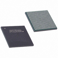
EP3C25F324I7 Altera, EP3C25F324I7 Datasheet - Page 154

EP3C25F324I7
Manufacturer Part Number
EP3C25F324I7
Description
IC CYCLONE III FPGA 25K 324 FBGA
Manufacturer
Altera
Series
Cyclone® IIIr
Datasheets
1.EP3C5F256C8N.pdf
(5 pages)
2.EP3C5F256C8N.pdf
(34 pages)
3.EP3C5F256C8N.pdf
(66 pages)
4.EP3C5F256C8N.pdf
(14 pages)
5.EP3C5F256C8N.pdf
(76 pages)
6.EP3C25F324I7.pdf
(274 pages)
Specifications of EP3C25F324I7
Number Of Logic Elements/cells
24624
Number Of Labs/clbs
1539
Total Ram Bits
608256
Number Of I /o
215
Voltage - Supply
1.15 V ~ 1.25 V
Mounting Type
Surface Mount
Operating Temperature
-40°C ~ 100°C
Package / Case
324-FBGA
Family Name
Cyclone III
Number Of Logic Blocks/elements
24624
# I/os (max)
215
Frequency (max)
437.5MHz
Process Technology
65nm
Operating Supply Voltage (typ)
1.2V
Logic Cells
24624
Ram Bits
608256
Operating Supply Voltage (min)
1.15V
Operating Supply Voltage (max)
1.25V
Operating Temp Range
-40C to 100C
Operating Temperature Classification
Industrial
Mounting
Surface Mount
Pin Count
324
Package Type
FBGA
For Use With
544-2370 - KIT STARTER CYCLONE III EP3C25
Lead Free Status / RoHS Status
Contains lead / RoHS non-compliant
Number Of Gates
-
Lead Free Status / Rohs Status
Not Compliant
Available stocks
Company
Part Number
Manufacturer
Quantity
Price
Company:
Part Number:
EP3C25F324I7N
Manufacturer:
ALTERA32
Quantity:
181
8–10
Address and Control/Command Pins
Memory Clock Pins
Cyclone III Device Family Memory Interfaces Features
DDR Input Registers
Cyclone III Device Handbook, Volume 1
1
1
Some DDR2 SDRAM and DDR SDRAM devices support error correction coding
(ECC), a method of detecting and automatically correcting errors in data
transmission. In 72-bit DDR2 or DDR SDRAM, there are eight ECC pins and 64 data
pins. Connect the DDR2 and DDR SDRAM ECC pins to a separate DQS or DQ group
in Cyclone III device family. The memory controller needs additional logic to encode
and decode the ECC data.
The address signals and the control or command signals are typically sent at a single
data rate. You can use any of the user I/O pins on all I/O banks of Cyclone III device
family to generate the address and control or command signals to the memory device.
Cyclone III device family does not support QDR II SRAM in the burst length of two.
In DDR2 and DDR SDRAM memory interfaces, the memory clock signals (CK and
CK#) are used to capture the address signals and the control or command signals.
Similarly, QDR II SRAM devices use the write clocks (K and K#) to capture the
address and command signals. The CK/CK# and K/K# signals are generated to
resemble the write-data strobe using the DDIO registers in Cyclone III device family.
CK/CK# pins must be placed on differential I/O pins and cannot be placed on the
same row or column as the DQ pins.
This section describes Cyclone III device family memory interfaces, including DDR
input registers, DDR output registers, OCT, and phase-lock loops (PLLs).
The DDR input registers are implemented with three internal logic element (LE)
registers for every DQ pin. These LE registers are located in the logic array block
(LAB) adjacent to the DDR input pin.
Chapter 8: External Memory Interfaces in the Cyclone III Device Family
Cyclone III Device Family Memory Interfaces Features
© January 2010 Altera Corporation


