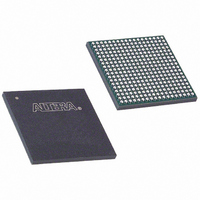
EP3C25F324I7 Altera, EP3C25F324I7 Datasheet - Page 145

EP3C25F324I7
Manufacturer Part Number
EP3C25F324I7
Description
IC CYCLONE III FPGA 25K 324 FBGA
Manufacturer
Altera
Series
Cyclone® IIIr
Datasheets
1.EP3C5F256C8N.pdf
(5 pages)
2.EP3C5F256C8N.pdf
(34 pages)
3.EP3C5F256C8N.pdf
(66 pages)
4.EP3C5F256C8N.pdf
(14 pages)
5.EP3C5F256C8N.pdf
(76 pages)
6.EP3C25F324I7.pdf
(274 pages)
Specifications of EP3C25F324I7
Number Of Logic Elements/cells
24624
Number Of Labs/clbs
1539
Total Ram Bits
608256
Number Of I /o
215
Voltage - Supply
1.15 V ~ 1.25 V
Mounting Type
Surface Mount
Operating Temperature
-40°C ~ 100°C
Package / Case
324-FBGA
Family Name
Cyclone III
Number Of Logic Blocks/elements
24624
# I/os (max)
215
Frequency (max)
437.5MHz
Process Technology
65nm
Operating Supply Voltage (typ)
1.2V
Logic Cells
24624
Ram Bits
608256
Operating Supply Voltage (min)
1.15V
Operating Supply Voltage (max)
1.25V
Operating Temp Range
-40C to 100C
Operating Temperature Classification
Industrial
Mounting
Surface Mount
Pin Count
324
Package Type
FBGA
For Use With
544-2370 - KIT STARTER CYCLONE III EP3C25
Lead Free Status / RoHS Status
Contains lead / RoHS non-compliant
Number Of Gates
-
Lead Free Status / Rohs Status
Not Compliant
Available stocks
Company
Part Number
Manufacturer
Quantity
Price
Company:
Part Number:
EP3C25F324I7N
Manufacturer:
ALTERA32
Quantity:
181
Figure 8–1. Cyclone III Device Family External Memory Data Path
Note to
(1) All clocks shown here are global clocks.
© January 2010 Altera Corporation
CIII51009-2.3
Figure
8–1:
f
PLL
1
-90° Shifted Clock
OE
In addition to an abundant supply of on-chip memory, Cyclone
(Cyclone III and Cyclone III LS devices) can easily interface to a broad range of
external memory, including DDR2 SDRAM, DDR SDRAM, and QDRII SRAM.
External memory devices are an important system component of a wide range of
image processing, storage, communications, and general embedded applications.
Altera
interfaces using the Altera ALTMEMPHY megafunction. You can implement the
controller function using the Altera DDR2 or DDR SDRAM memory controllers,
third-party controllers, or a custom controller for unique application needs.
Cyclone III device family supports QDR II interfaces electrically, but Altera does not
supply controller or physical layer (PHY) megafunctions for QDR II interfaces.
This chapter includes a description of the hardware interfaces for external memory
interfaces available in Cyclone III device family.
This chapter contains the following sections:
■
■
For more information about external memory system performance specifications,
board design guidelines, timing analysis, simulation, and debugging information,
refer to
Figure 8–1
in Cyclone III device family.
Register
System Clock
IOE
Register
“Cyclone III Device Family Memory Interfaces Pin Support” on page 8–2
“Cyclone III Device Family Memory Interfaces Features” on page 8–10
IOE
®
GND
V CC
recommends that you construct all DDR2 or DDR SDRAM external memory
Literature: External Memory
Capture Clock
shows the block diagram of a typical external memory interface data path
Register
Register
IOE
IOE
DQS/CQ/CQn
8. External Memory Interfaces in the
OE
Register
IOE
Register
Interfaces.
IOE
(Note 1)
DataA
DataB
Register
Register
Cyclone III Device Family
IOE
IOE
DQ
Cyclone III Device Handbook, Volume 1
Register
Register
®
LE
LE
III device family
Register
LE


