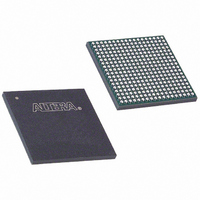
EP3C25F324I7 Altera, EP3C25F324I7 Datasheet - Page 94

EP3C25F324I7
Manufacturer Part Number
EP3C25F324I7
Description
IC CYCLONE III FPGA 25K 324 FBGA
Manufacturer
Altera
Series
Cyclone® IIIr
Datasheets
1.EP3C5F256C8N.pdf
(5 pages)
2.EP3C5F256C8N.pdf
(34 pages)
3.EP3C5F256C8N.pdf
(66 pages)
4.EP3C5F256C8N.pdf
(14 pages)
5.EP3C5F256C8N.pdf
(76 pages)
6.EP3C25F324I7.pdf
(274 pages)
Specifications of EP3C25F324I7
Number Of Logic Elements/cells
24624
Number Of Labs/clbs
1539
Total Ram Bits
608256
Number Of I /o
215
Voltage - Supply
1.15 V ~ 1.25 V
Mounting Type
Surface Mount
Operating Temperature
-40°C ~ 100°C
Package / Case
324-FBGA
Family Name
Cyclone III
Number Of Logic Blocks/elements
24624
# I/os (max)
215
Frequency (max)
437.5MHz
Process Technology
65nm
Operating Supply Voltage (typ)
1.2V
Logic Cells
24624
Ram Bits
608256
Operating Supply Voltage (min)
1.15V
Operating Supply Voltage (max)
1.25V
Operating Temp Range
-40C to 100C
Operating Temperature Classification
Industrial
Mounting
Surface Mount
Pin Count
324
Package Type
FBGA
For Use With
544-2370 - KIT STARTER CYCLONE III EP3C25
Lead Free Status / RoHS Status
Contains lead / RoHS non-compliant
Number Of Gates
-
Lead Free Status / Rohs Status
Not Compliant
Available stocks
Company
Part Number
Manufacturer
Quantity
Price
Company:
Part Number:
EP3C25F324I7N
Manufacturer:
ALTERA32
Quantity:
181
5–30
Table 5–9. Dynamic Phase Shifting Control Signals
Cyclone III Device Handbook, Volume 1
PHASECOUNTERSELECT[2:0]
PHASEUPDOWN
PHASESTEP
SCANCLK
PHASEDONE
Signal Name
Table 5–8
PLLs.
Table 5–8. PLL Counter Settings
To bypass any of the PLL counters, set the bypass bit to 1. The values on the other bits
are then ignored.
Dynamic Phase Shifting
The dynamic phase shifting feature allows the output phase of individual PLL
outputs to be dynamically adjusted relative to each other and the reference clock
without sending serial data through the scan chain of the corresponding PLL. This
feature simplifies the interface and allows you to quickly adjust t
changing output clock phase shift in real time. This is achieved by incrementing or
decrementing the VCO phase-tap selection to a given C counter or to the M counter.
The phase is shifted by 1/8 the VCO frequency at a time. The output clocks are active
during this phase reconfiguration process.
Table 5–9
Note to
(1) Bypass bit.
X
X
Table
X
X
lists the settings for bypassing the counters in Cyclone III device family
lists the control signals that are used for dynamic phase shifting.
PLL Scan Chain Bits [0..8] Settings
5–8:
Counter Select. Three bits decoded to select
either the M or one of the C counters for
phase adjustment. One address map to select
all C counters. This signal is registered in the
PLL on the rising edge of SCANCLK.
Selects dynamic phase shift direction; 1= UP,
0 = DOWN. Signal is registered in the PLL on
the rising edge of SCANCLK.
Logic high enables dynamic phase shifting.
Free running clock from core used in
combination with PHASESTEP to enable or
disable dynamic phase shifting. Shared with
SCANCLK for dynamic reconfiguration.
When asserted, it indicates to core logic that
the phase adjustment is complete and PLL is
ready to act on a possible second adjustment
pulse. Asserts based on internal PLL timing.
Deasserts on rising edge of SCANCLK.
X
X
X
X
LSB
X
X
Description
X
X
Chapter 5: Clock Networks and PLLs in the Cyclone III Device Family
X
X
X
X
1
0
MSB
(1)
(1)
Logic array or I/O
pins
Logic array or I/O
pins
Logic array or I/O
pins
GCLK or I/O pins
PLL reconfiguration
circuit
PLL counter bypassed
PLL counter not bypassed
© December 2009 Altera Corporation
Source
Description
CO
delays by
PLL Reconfiguration
PLL
reconfiguration
circuit
PLL
reconfiguration
circuit
PLL
reconfiguration
circuit
PLL
reconfiguration
circuit
Logic array or
I/O pins
Destination


