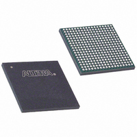
EP3C25F324I7 Altera, EP3C25F324I7 Datasheet - Page 92

EP3C25F324I7
Manufacturer Part Number
EP3C25F324I7
Description
IC CYCLONE III FPGA 25K 324 FBGA
Manufacturer
Altera
Series
Cyclone® IIIr
Datasheets
1.EP3C5F256C8N.pdf
(5 pages)
2.EP3C5F256C8N.pdf
(34 pages)
3.EP3C5F256C8N.pdf
(66 pages)
4.EP3C5F256C8N.pdf
(14 pages)
5.EP3C5F256C8N.pdf
(76 pages)
6.EP3C25F324I7.pdf
(274 pages)
Specifications of EP3C25F324I7
Number Of Logic Elements/cells
24624
Number Of Labs/clbs
1539
Total Ram Bits
608256
Number Of I /o
215
Voltage - Supply
1.15 V ~ 1.25 V
Mounting Type
Surface Mount
Operating Temperature
-40°C ~ 100°C
Package / Case
324-FBGA
Family Name
Cyclone III
Number Of Logic Blocks/elements
24624
# I/os (max)
215
Frequency (max)
437.5MHz
Process Technology
65nm
Operating Supply Voltage (typ)
1.2V
Logic Cells
24624
Ram Bits
608256
Operating Supply Voltage (min)
1.15V
Operating Supply Voltage (max)
1.25V
Operating Temp Range
-40C to 100C
Operating Temperature Classification
Industrial
Mounting
Surface Mount
Pin Count
324
Package Type
FBGA
For Use With
544-2370 - KIT STARTER CYCLONE III EP3C25
Lead Free Status / RoHS Status
Contains lead / RoHS non-compliant
Number Of Gates
-
Lead Free Status / Rohs Status
Not Compliant
Available stocks
Company
Part Number
Manufacturer
Quantity
Price
Company:
Part Number:
EP3C25F324I7N
Manufacturer:
ALTERA32
Quantity:
181
5–28
Figure 5–23. Scan Chain Bit Order
Cyclone III Device Handbook, Volume 1
DATAOUT
HB
LB
0
0
HB
Table 5–4. Cyclone III Device Family PLL Reprogramming Bits (Part 2 of 2)
Figure 5–22
Figure 5–22. PLL Component Scan Chain Order
Figure 5–23
Cyclone III device family PLLs.
LB
1
1
N
Charge Pump
Loop Filter
Total number of bits:
Notes to
(1) LSB bit for C4 low-count value is the first bit shifted into the scan chain.
(2) These two control bits include rbypass, for bypassing the counter, and rselodd, to select the output clock
(3) MSB bit for loop filter is the last bit shifted into the scan chain.
Block Name
duty cycle.
DATAIN
HB
Table
LB
2
2
(3)
shows the scan chain order of the PLL components.
shows the scan chain bit order sequence for one PLL post-scale counter in
5–4:
HB
LB
3
3
DATAOUT
MSB
HB
LB
4
4
Counter
LF
16
9
9
HB
CP
LB
5
5
Chapter 5: Clock Networks and PLLs in the Cyclone III Device Family
C4
LSB
HB
LB
6
6
Number of Bits
HB
LB
7
7
C3
N
Other
2
0
0
(2)
HB
LB
8
8
© December 2009 Altera Corporation
C2
M
LB
HB
9
9
PLL Reconfiguration
rselodd
Total
C0
C1
rbypass
144
18
9
9
DATAIN


