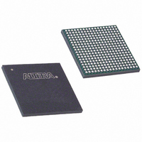
EP3C25F324I7 Altera, EP3C25F324I7 Datasheet - Page 96

EP3C25F324I7
Manufacturer Part Number
EP3C25F324I7
Description
IC CYCLONE III FPGA 25K 324 FBGA
Manufacturer
Altera
Series
Cyclone® IIIr
Datasheets
1.EP3C5F256C8N.pdf
(5 pages)
2.EP3C5F256C8N.pdf
(34 pages)
3.EP3C5F256C8N.pdf
(66 pages)
4.EP3C5F256C8N.pdf
(14 pages)
5.EP3C5F256C8N.pdf
(76 pages)
6.EP3C25F324I7.pdf
(274 pages)
Specifications of EP3C25F324I7
Number Of Logic Elements/cells
24624
Number Of Labs/clbs
1539
Total Ram Bits
608256
Number Of I /o
215
Voltage - Supply
1.15 V ~ 1.25 V
Mounting Type
Surface Mount
Operating Temperature
-40°C ~ 100°C
Package / Case
324-FBGA
Family Name
Cyclone III
Number Of Logic Blocks/elements
24624
# I/os (max)
215
Frequency (max)
437.5MHz
Process Technology
65nm
Operating Supply Voltage (typ)
1.2V
Logic Cells
24624
Ram Bits
608256
Operating Supply Voltage (min)
1.15V
Operating Supply Voltage (max)
1.25V
Operating Temp Range
-40C to 100C
Operating Temperature Classification
Industrial
Mounting
Surface Mount
Pin Count
324
Package Type
FBGA
For Use With
544-2370 - KIT STARTER CYCLONE III EP3C25
Lead Free Status / RoHS Status
Contains lead / RoHS non-compliant
Number Of Gates
-
Lead Free Status / Rohs Status
Not Compliant
Available stocks
Company
Part Number
Manufacturer
Quantity
Price
Company:
Part Number:
EP3C25F324I7N
Manufacturer:
ALTERA32
Quantity:
181
5–32
Spread-Spectrum Clocking
PLL Specifications
Cyclone III Device Handbook, Volume 1
f
f
The phasestep signal is latched on the negative edge of scanclk. In
this is shown by the second scanclk falling edge. phasestep must stay high for at
least two scanclk cycles. On the second scanclk rising edge after phasestep is
latched (indicated by the fourth rising edge), the values of phaseupdown and
phasecounterselect are latched and the PLL starts dynamic phase shifting for the
specified counter or counters and in the indicated direction. On the fourth scanclk
rising edge, phasedone goes high to low and remains low until the PLL finishes
dynamic phase shifting. You can perform another dynamic phase shift after the
phasedone signal goes from low to high.
Depending on the VCO and scanclk frequencies, phasedone low time may be
greater than or less than one scanclk cycle. The maximum time for reconfiguring
phase shift dynamically is to be determined (TBD) based on device characterization.
After phasedone goes from low to high, you can perform another dynamic phase
shift. phasestep pulses must be at least one scanclk cycle apart.
For information about the ALTPLL_RECONFIG MegaWizard Plug-In Manager, refer
to the
The Cyclone III device family can accept a spread-spectrum input with typical
modulation frequencies. However, the device cannot automatically detect that the
input is a spread-spectrum signal. Instead, the input signal looks like deterministic
jitter at the input of the PLL. Cyclone III device family PLLs can track a
spread-spectrum input clock as long as it is in the input jitter tolerance specifications
and the modulation frequency of the input clock is below the PLL bandwidth, which
is specified in the fitter report. The Cyclone III device family cannot generate
spread-spectrum signals internally.
For information about PLL specifications, refer to the
Cyclone III LS Device Data Sheet
ALTPLL_RECONFIG Megafunction User
chapters.
Chapter 5: Clock Networks and PLLs in the Cyclone III Device Family
Guide.
Cyclone III Device Data Sheet
© December 2009 Altera Corporation
Spread-Spectrum Clocking
Figure
5–24,
and


