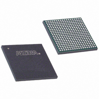
EP3C25F324I7 Altera, EP3C25F324I7 Datasheet - Page 269

EP3C25F324I7
Manufacturer Part Number
EP3C25F324I7
Description
IC CYCLONE III FPGA 25K 324 FBGA
Manufacturer
Altera
Series
Cyclone® IIIr
Datasheets
1.EP3C5F256C8N.pdf
(5 pages)
2.EP3C5F256C8N.pdf
(34 pages)
3.EP3C5F256C8N.pdf
(66 pages)
4.EP3C5F256C8N.pdf
(14 pages)
5.EP3C5F256C8N.pdf
(76 pages)
6.EP3C25F324I7.pdf
(274 pages)
Specifications of EP3C25F324I7
Number Of Logic Elements/cells
24624
Number Of Labs/clbs
1539
Total Ram Bits
608256
Number Of I /o
215
Voltage - Supply
1.15 V ~ 1.25 V
Mounting Type
Surface Mount
Operating Temperature
-40°C ~ 100°C
Package / Case
324-FBGA
Family Name
Cyclone III
Number Of Logic Blocks/elements
24624
# I/os (max)
215
Frequency (max)
437.5MHz
Process Technology
65nm
Operating Supply Voltage (typ)
1.2V
Logic Cells
24624
Ram Bits
608256
Operating Supply Voltage (min)
1.15V
Operating Supply Voltage (max)
1.25V
Operating Temp Range
-40C to 100C
Operating Temperature Classification
Industrial
Mounting
Surface Mount
Pin Count
324
Package Type
FBGA
For Use With
544-2370 - KIT STARTER CYCLONE III EP3C25
Lead Free Status / RoHS Status
Contains lead / RoHS non-compliant
Number Of Gates
-
Lead Free Status / Rohs Status
Not Compliant
Available stocks
Company
Part Number
Manufacturer
Quantity
Price
Company:
Part Number:
EP3C25F324I7N
Manufacturer:
ALTERA32
Quantity:
181
Chapter 12: IEEE 1149.1 (JTAG) Boundary-Scan Testing for the Cyclone III Device Family
IEEE Std. 1149.1 BST Operation Control
Table 12–3. IEEE Std. 1149.1 (JTAG) Instructions Supported by Cyclone III Device Family (Part 1 of 2)
© December 2009
SAMPLE/PRELOAD
EXTEST
BYPASS
USERCODE
IDCODE
HIGHZ
CLAMP
ICR Instructions
PULSE_NCONFIG
CONFIG_IO
EN_ACTIVE_CLK
DIS_ACTIVE_CLK
ACTIVE_DISENGAGE
ACTIVE_ENGAGE
JTAG Instruction
(1)
(2)
Altera Corporation
(2)
(2)
(2)
Cyclone III device family supports the IEEE Std. 1149.1 (JTAG) instructions as listed in
Table
(2)
12–3.
Instruction Code
00 0000 0101
00 0000 1111
11 1111 1111
00 0000 0111
00 0000 1011
00 0000 1010
00 0000 0001
00 0000 1101
01 1110 1110
10 1110 1110
10 1101 0000
10 1011 0000
00 000 0110
—
Allows a snapshot of signals at the device pins to be captured and
examined during normal device operation, and permits an initial data
pattern to be output at the device pins. Also used by the SignalTap
embedded logic analyzer.
Allows the external circuitry and board-level interconnects to be tested
by forcing a test pattern at the output pins and capturing test results at
the input pins.
Places the 1-bit bypass register between the TDI and TDO pins, which
allows the BST data to pass synchronously through selected devices to
adjacent devices during normal device operation.
Selects the 32-bit USERCODE register and places it between the TDI
and TDO pins, allowing the USERCODE to be serially shifted out of
TDO.
Selects the IDCODE register and places it between TDI and TDO,
allowing the IDCODE to be serially shifted out of TDO. IDCODE is the
default instruction at power up and in TAP RESET state.
Places the 1-bit bypass register between the TDI and TDO pins, which
allows the BST data to pass synchronously through selected devices to
adjacent devices during normal device operation, while tri-stating all of
the I/O pins.
Places the 1-bit bypass register between the TDI and TDO pins, which
allows the BST data to pass synchronously through selected devices to
adjacent devices during normal device operation while holding I/O pins
to a state defined by the data in the boundary scan register.
Used when configuring Cyclone III device family using the JTAG port
with a USB-Blaster
download cable, or when using a Jam File, or JBC File via an embedded
processor.
Emulates pulsing the nCONFIG pin low to trigger reconfiguration even
though the physical pin is unaffected.
Allows I/O reconfiguration through JTAG ports using the IOCSR for
JTAG testing. This is executed after or during configurations.
nSTATUS pin must go high before you can issue the CONFIG_IO
instruction.
Allows CLKUSR pin signal to replace the internal oscillator as the
configuration clock source.
Allows you to revert the configuration clock source from CLKUSR pin
signal set by EN_ACTIVE_CLK back to the internal oscillator.
Places the active configuration mode controllers into idle state prior to
CONFIG_IO to configure the IOCSR or perform board level testing.
This instruction might be used in AS and AP configuration schemes to
re-engage the active controller.
™
ByteBlaster
Description
™
II, MasterBlaster
Cyclone III Device Handbook, Volume 1
™
or ByteBlasterMV
®
II
12–3
™


