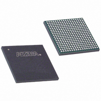
EP3C25F324I7 Altera, EP3C25F324I7 Datasheet - Page 271

EP3C25F324I7
Manufacturer Part Number
EP3C25F324I7
Description
IC CYCLONE III FPGA 25K 324 FBGA
Manufacturer
Altera
Series
Cyclone® IIIr
Datasheets
1.EP3C5F256C8N.pdf
(5 pages)
2.EP3C5F256C8N.pdf
(34 pages)
3.EP3C5F256C8N.pdf
(66 pages)
4.EP3C5F256C8N.pdf
(14 pages)
5.EP3C5F256C8N.pdf
(76 pages)
6.EP3C25F324I7.pdf
(274 pages)
Specifications of EP3C25F324I7
Number Of Logic Elements/cells
24624
Number Of Labs/clbs
1539
Total Ram Bits
608256
Number Of I /o
215
Voltage - Supply
1.15 V ~ 1.25 V
Mounting Type
Surface Mount
Operating Temperature
-40°C ~ 100°C
Package / Case
324-FBGA
Family Name
Cyclone III
Number Of Logic Blocks/elements
24624
# I/os (max)
215
Frequency (max)
437.5MHz
Process Technology
65nm
Operating Supply Voltage (typ)
1.2V
Logic Cells
24624
Ram Bits
608256
Operating Supply Voltage (min)
1.15V
Operating Supply Voltage (max)
1.25V
Operating Temp Range
-40C to 100C
Operating Temperature Classification
Industrial
Mounting
Surface Mount
Pin Count
324
Package Type
FBGA
For Use With
544-2370 - KIT STARTER CYCLONE III EP3C25
Lead Free Status / RoHS Status
Contains lead / RoHS non-compliant
Number Of Gates
-
Lead Free Status / Rohs Status
Not Compliant
Available stocks
Company
Part Number
Manufacturer
Quantity
Price
Company:
Part Number:
EP3C25F324I7N
Manufacturer:
ALTERA32
Quantity:
181
Chapter 12: IEEE 1149.1 (JTAG) Boundary-Scan Testing for the Cyclone III Device Family
I/O Voltage Support in a JTAG Chain
I/O Voltage Support in a JTAG Chain
© December 2009
f
1
Altera Corporation
For more information about the following topics, refer to
Boundary-Scan Testing in Altera
■
■
■
■
■
The following information is only applicable to Cyclone III LS devices:
■
■
■
A JTAG chain can contain several different devices. However, you must be cautious if
the chain contains devices that have different V
the TDO pin must meet the specifications of the TDI pin it drives. For Cyclone III
device family, the TDO pin is powered by the V
supply is 3.3 V, the TDO pin drives out 3.3 V.
Devices can interface with each other although they might have different V
For example, a device with a 3.3-V TDO pin can drive to a device with a 5.0-V TDI pin
because 3.3 V meets the minimum TTL-level V
Cyclone III device family can support 2.5-V or 3.3-V input levels.
For multiple devices in a JTAG chain with 3.0-V or 3.3-V I/O standard, you must
connect a 25-Ω series resistor on a TDO pin driving a TDI pin.
You can also interface the TDI and TDO lines of the devices that have different V
levels by inserting a level shifter between the devices. If possible, the JTAG chain must
be built in such a way that a device with a higher V
equal or lower V
TDO level to a level acceptable to the JTAG tester.
TAP controller state-machine
Timing requirements for IEEE Std. 1149.1 signals
Instruction mode
Mandatory JTAG instructions (SAMPLE/PRELOAD, EXTEST and BYPASS)
Optional JTAG instructions (IDCODE, USERCODE, CLAMP and HIGHZ)
Only the three mandatory JTAG 1149.1 JTAG instructions (BYPASS,
SAMPLE/PRELOAD, EXTEST) and the FACTORY private instruction are supported
from the JTAG pins upon power up. The FACTORY instruction (instruction code:
10 1000 0001) must be issued before the device starts loading the core
configuration data to enable access to all other JTAG instructions. This instruction
also clears the device configuration data and AES volatile key.
IDCODE instruction is not supported upon power-up, prior to issuing the
FACTORY instruction. However, it is the default instruction when the TAP
controller is in the reset state. Without loading any instructions, you can go to the
Shift_DR state and shift out the JTAG Device ID.
IDCODE, CONFIG_IO, ACTIVE_DISENGAGE, HIGHZ, CLAMP, USERCODE and
PULSE_NCONFIG instructions are supported, provided that the FACTORY
instruction is executed.
CCIO
level. This way, a level shifter may be required only to shift the
Devices:
CCIO
IH
CCIO
for the 5.0-V TDI pin. JTAG pins on
power supply. Because the V
CCIO
levels. The output voltage level of
level drives to a device with an
AN39: IEEE 1149.1 (JTAG)
Cyclone III Device Handbook, Volume 1
CCIO
levels.
CCIO
CCIO
12–5


