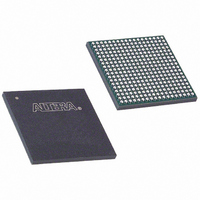
EP3C25F324I7 Altera, EP3C25F324I7 Datasheet - Page 38

EP3C25F324I7
Manufacturer Part Number
EP3C25F324I7
Description
IC CYCLONE III FPGA 25K 324 FBGA
Manufacturer
Altera
Series
Cyclone® IIIr
Datasheets
1.EP3C5F256C8N.pdf
(5 pages)
2.EP3C5F256C8N.pdf
(34 pages)
3.EP3C5F256C8N.pdf
(66 pages)
4.EP3C5F256C8N.pdf
(14 pages)
5.EP3C5F256C8N.pdf
(76 pages)
6.EP3C25F324I7.pdf
(274 pages)
Specifications of EP3C25F324I7
Number Of Logic Elements/cells
24624
Number Of Labs/clbs
1539
Total Ram Bits
608256
Number Of I /o
215
Voltage - Supply
1.15 V ~ 1.25 V
Mounting Type
Surface Mount
Operating Temperature
-40°C ~ 100°C
Package / Case
324-FBGA
Family Name
Cyclone III
Number Of Logic Blocks/elements
24624
# I/os (max)
215
Frequency (max)
437.5MHz
Process Technology
65nm
Operating Supply Voltage (typ)
1.2V
Logic Cells
24624
Ram Bits
608256
Operating Supply Voltage (min)
1.15V
Operating Supply Voltage (max)
1.25V
Operating Temp Range
-40C to 100C
Operating Temperature Classification
Industrial
Mounting
Surface Mount
Pin Count
324
Package Type
FBGA
For Use With
544-2370 - KIT STARTER CYCLONE III EP3C25
Lead Free Status / RoHS Status
Contains lead / RoHS non-compliant
Number Of Gates
-
Lead Free Status / Rohs Status
Not Compliant
Available stocks
Company
Part Number
Manufacturer
Quantity
Price
Company:
Part Number:
EP3C25F324I7N
Manufacturer:
ALTERA32
Quantity:
181
3–2
Cyclone III Device Handbook, Volume 1
f
Table 3–1
Table 3–1. Summary of M9K Memory Features
For information about the number of M9K memory blocks for the Cyclone III device
family, refer to the
Configurations (depth × width)
Parity bits
Byte enable
Packed mode
Address clock enable
Single-port mode
Simple dual-port mode
True dual-port mode
Embedded shift register mode
ROM mode
FIFO buffer
Simple dual-port mixed width support
True dual-port mixed width support
Memory initialization file (.mif)
Mixed-clock mode
Power-up condition
Register asynchronous clears
Latch asynchronous clears
Write or read operation triggering
Same-port read-during-write
Mixed-port read-during-write
Notes to
(1) FIFO buffers and embedded shift registers that require external logic elements (LEs) for implementing control
(2) Width modes of ×32 and ×36 are not available.
logic.
Table
lists the features supported by the M9K memory
(1)
3–1:
Feature
Cyclone III Device Family Overview
(1)
(2)
Read address registers and output registers only
Chapter 3: Memory Blocks in the Cyclone III Device Family
Outputs set to Old Data or Don’t Care
Outputs set to Old Data or New Data
Write and read: Rising clock edges
chapter.
Output latches only
Outputs cleared
M9K Blocks
© December 2009 Altera Corporation
8192 × 1
4096 × 2
2048 × 4
1024 × 8
1024 × 9
512 × 16
512 × 18
256 × 32
256 × 36
v
v
v
v
v
v
v
v
v
v
v
v
v
v
Overview


