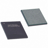
EP3C25F324I7 Altera, EP3C25F324I7 Datasheet - Page 127

EP3C25F324I7
Manufacturer Part Number
EP3C25F324I7
Description
IC CYCLONE III FPGA 25K 324 FBGA
Manufacturer
Altera
Series
Cyclone® IIIr
Datasheets
1.EP3C5F256C8N.pdf
(5 pages)
2.EP3C5F256C8N.pdf
(34 pages)
3.EP3C5F256C8N.pdf
(66 pages)
4.EP3C5F256C8N.pdf
(14 pages)
5.EP3C5F256C8N.pdf
(76 pages)
6.EP3C25F324I7.pdf
(274 pages)
Specifications of EP3C25F324I7
Number Of Logic Elements/cells
24624
Number Of Labs/clbs
1539
Total Ram Bits
608256
Number Of I /o
215
Voltage - Supply
1.15 V ~ 1.25 V
Mounting Type
Surface Mount
Operating Temperature
-40°C ~ 100°C
Package / Case
324-FBGA
Family Name
Cyclone III
Number Of Logic Blocks/elements
24624
# I/os (max)
215
Frequency (max)
437.5MHz
Process Technology
65nm
Operating Supply Voltage (typ)
1.2V
Logic Cells
24624
Ram Bits
608256
Operating Supply Voltage (min)
1.15V
Operating Supply Voltage (max)
1.25V
Operating Temp Range
-40C to 100C
Operating Temperature Classification
Industrial
Mounting
Surface Mount
Pin Count
324
Package Type
FBGA
For Use With
544-2370 - KIT STARTER CYCLONE III EP3C25
Lead Free Status / RoHS Status
Contains lead / RoHS non-compliant
Number Of Gates
-
Lead Free Status / Rohs Status
Not Compliant
Available stocks
Company
Part Number
Manufacturer
Quantity
Price
Company:
Part Number:
EP3C25F324I7N
Manufacturer:
ALTERA32
Quantity:
181
Chapter 7: High-Speed Differential Interfaces in the Cyclone III Device Family
High-Speed I/O Interface
Table 7–1. Differential I/O Standards Supported in Cyclone III Device Family I/O Banks
© December 2009
LVDS
RSDS
mini-LVDS
PPDS
BLVDS
LVPECL
Differential SSTL-2
Differential SSTL-18
Differential HSTL-18
Differential HSTL-15
Differential HSTL-12
Notes to
(1) Transmitter and Receiver F
(2) The LVPECL I/O standard is only supported on dedicated clock input pins.
(3) The differential SSTL-2, SSTL-18, HSTL-18, HSTL-15, and HSTL-12 I/O standards are only supported on clock input pins and PLL output clock
Differential I/O Standards
pins. PLL output clock pins do not support Class II interface type of differential SSTL-18, HSTL-18, HSTL-15, and HSTL-12 I/O standards.
(1)
Table
(2)
7–1:
Altera Corporation
(3)
(3)
(3)
(3)
(3)
Table 7–1
family.
You can use I/O pins and internal logic to implement a high-speed differential
interface in the Cyclone III device family. The Cyclone III device family does not
contain dedicated serialization or deserialization circuitry. Therefore, shift registers,
internal phase-locked loops (PLLs), and I/O cells are used to perform
serial-to-parallel conversions on incoming data and parallel-to-serial conversion on
outgoing data. The differential interface data serializers and deserializers (SERDES)
are automatically constructed in the core logic elements (LEs) with the Quartus
software ALTLVDS megafunction.
MAX
depend on system topology and performance requirement.
lists which I/O bank supports these I/O standards in the Cyclone III device
I/O Bank Location
3, 4, 7, 8
1,2,5,6
1,2,5,6
1,2,5,6
1,2,5,6
All
All
All
All
All
All
All
All
All
All
All
External Resistor
Three Resistors
Three Resistors
Three Resistors
Three Resistors
Single Resistor
Single Resistor
Not Required
Not Required
Not Required
Not Required
Transmitter
Network at
NA
NA
NA
NA
NA
NA
Transmitter (TX)
Cyclone III Device Handbook, Volume 1
Supported
Yes
Yes
Yes
Yes
Yes
Not
Yes
Yes
Yes
Yes
Yes
Receiver (RX)
Supported
Supported
Supported
Yes
Not
Not
Not
Yes
Yes
Yes
Yes
Yes
Yes
Yes
®
II
7–3


