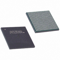
EP3C25F324I7 Altera, EP3C25F324I7 Datasheet - Page 172

EP3C25F324I7
Manufacturer Part Number
EP3C25F324I7
Description
IC CYCLONE III FPGA 25K 324 FBGA
Manufacturer
Altera
Series
Cyclone® IIIr
Datasheets
1.EP3C5F256C8N.pdf
(5 pages)
2.EP3C5F256C8N.pdf
(34 pages)
3.EP3C5F256C8N.pdf
(66 pages)
4.EP3C5F256C8N.pdf
(14 pages)
5.EP3C5F256C8N.pdf
(76 pages)
6.EP3C25F324I7.pdf
(274 pages)
Specifications of EP3C25F324I7
Number Of Logic Elements/cells
24624
Number Of Labs/clbs
1539
Total Ram Bits
608256
Number Of I /o
215
Voltage - Supply
1.15 V ~ 1.25 V
Mounting Type
Surface Mount
Operating Temperature
-40°C ~ 100°C
Package / Case
324-FBGA
Family Name
Cyclone III
Number Of Logic Blocks/elements
24624
# I/os (max)
215
Frequency (max)
437.5MHz
Process Technology
65nm
Operating Supply Voltage (typ)
1.2V
Logic Cells
24624
Ram Bits
608256
Operating Supply Voltage (min)
1.15V
Operating Supply Voltage (max)
1.25V
Operating Temp Range
-40C to 100C
Operating Temperature Classification
Industrial
Mounting
Surface Mount
Pin Count
324
Package Type
FBGA
For Use With
544-2370 - KIT STARTER CYCLONE III EP3C25
Lead Free Status / RoHS Status
Contains lead / RoHS non-compliant
Number Of Gates
-
Lead Free Status / Rohs Status
Not Compliant
Available stocks
Company
Part Number
Manufacturer
Quantity
Price
Company:
Part Number:
EP3C25F324I7N
Manufacturer:
ALTERA32
Quantity:
181
9–12
Table 9–7. Cyclone III Device Family Configuration Schemes
AS Configuration (Serial Configuration Devices)
Cyclone III Device Handbook, Volume 1
Fast Passive Parallel Fast (FPP Fast POR)
with Encryption (for Cyclone III LS
devices only)
JTAG-based configuration
Notes to
(1) Altera recommends connecting the MSEL pins to V
(2) The configuration voltage standard is applied to the V
(3) You must follow specific requirements when interfacing Cyclone III device family with 2.5-, 3.0-, and 3.3-V configuration voltage standards. For
(4) FPP configuration is not supported in the Cyclone III E144 device package of Cyclone III devices.
(5) The JTAG-based configuration takes precedence over other configuration schemes, which means the MSEL pin settings are ignored.
(6) Do not leave the MSEL pins floating. Connect them to V
more information about these requirements, refer to
Altera recommends connecting the MSEL pins to GND if your device is only using the JTAG configuration.
Table
Configuration Scheme
f
9–7:
In the AS configuration scheme, Cyclone III device family is configured using a serial
configuration device. These configuration devices are low-cost devices with
non-volatile memories that feature a simple four-pin interface and a small form factor.
These features make serial configuration devices the ideal low-cost configuration
solution.
For more information about serial configuration devices, refer to the
Configuration Devices (EPCS1, EPCS4, EPCS16, EPCS64, and EPCS128) Data Sheet
chapter in volume 2 of the Configuration Handbook.
In Cyclone III device family, the active master clock frequency runs at a maximum of
40 MHz, and typically at 30 MHz. Cyclone III device family only work with serial
configuration devices that support up to 40 MHz.
Serial configuration devices provide a serial interface to access configuration data.
During device configuration, Cyclone III device family reads configuration data using
the serial interface, decompress data if necessary, and configure their SRAM cells. This
scheme is referred to as the AS configuration scheme because the device controls the
configuration interface.
Single-Device AS Configuration
The four-pin interface of serial configuration devices consists of the following pins:
■
■
■
■
This four-pin interface connects to Cyclone III device family pins, as shown in
Figure
(5)
Serial clock input (DCLK)
Serial data output (DATA)
AS data input (ASDI)
Active-low chip select (nCS)
9–3.
Chapter 9: Configuration, Design Security, and Remote System Upgrades in the Cyclone III Device Family
CCA
“Configuration and JTAG Pin I/O Requirements” on page
CCIO
(6)
CCA
or GND depending on the MSEL pin settings.
3
0
supply of the bank in which the configuration pins reside.
or GND. These pins support the non-JTAG configuration scheme used in production.
(6)
2
1
MSEL
(Note 1)
(6)
1
1
(Part 2 of 2)
(6)
0
0
Configuration Voltage Standard (V)
© December 2009 Altera Corporation
9–7.
(2),(3)
1.8/1.5
—
Serial
Configuration Features


