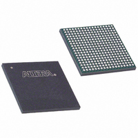
EP3C25F324I7 Altera, EP3C25F324I7 Datasheet - Page 257

EP3C25F324I7
Manufacturer Part Number
EP3C25F324I7
Description
IC CYCLONE III FPGA 25K 324 FBGA
Manufacturer
Altera
Series
Cyclone® IIIr
Datasheets
1.EP3C5F256C8N.pdf
(5 pages)
2.EP3C5F256C8N.pdf
(34 pages)
3.EP3C5F256C8N.pdf
(66 pages)
4.EP3C5F256C8N.pdf
(14 pages)
5.EP3C5F256C8N.pdf
(76 pages)
6.EP3C25F324I7.pdf
(274 pages)
Specifications of EP3C25F324I7
Number Of Logic Elements/cells
24624
Number Of Labs/clbs
1539
Total Ram Bits
608256
Number Of I /o
215
Voltage - Supply
1.15 V ~ 1.25 V
Mounting Type
Surface Mount
Operating Temperature
-40°C ~ 100°C
Package / Case
324-FBGA
Family Name
Cyclone III
Number Of Logic Blocks/elements
24624
# I/os (max)
215
Frequency (max)
437.5MHz
Process Technology
65nm
Operating Supply Voltage (typ)
1.2V
Logic Cells
24624
Ram Bits
608256
Operating Supply Voltage (min)
1.15V
Operating Supply Voltage (max)
1.25V
Operating Temp Range
-40C to 100C
Operating Temperature Classification
Industrial
Mounting
Surface Mount
Pin Count
324
Package Type
FBGA
For Use With
544-2370 - KIT STARTER CYCLONE III EP3C25
Lead Free Status / RoHS Status
Contains lead / RoHS non-compliant
Number Of Gates
-
Lead Free Status / Rohs Status
Not Compliant
Available stocks
Company
Part Number
Manufacturer
Quantity
Price
Company:
Part Number:
EP3C25F324I7N
Manufacturer:
ALTERA32
Quantity:
181
Chapter 11: SEU Mitigation in the Cyclone III Device Family
Automated SEU Detection
Table 11–1. CHANGE_EDREG JTAG Instruction
Automated SEU Detection
CRC_ERROR Pin
Table 11–2. CRC_ERROR Pin Description
© December 2009
Cyclone III
Cyclone III LS
CHANGE_EDREG
JTAG Instruction
Device
1
Altera Corporation
CRC_ERROR
Open Drain
Open Drain
(Optional)
Dedicated
Output or
Pin Type
Output
Output
Instruction Code
Table 11–1
00 0001 0101
After the test completes, Altera recommends that you power cycle the device.
Cyclone III device family offers on-chip circuitry for automated checking of SEU
detection. Applications that require the device to operate error-free at high elevations
or in close proximity to earth’s North or South Pole require periodic checks to ensure
continued data integrity. The error detection cyclic redundancy code feature
controlled by the Device and Pin Options dialog box in the Quartus II software uses a
32-bit CRC circuit to ensure data reliability and is one of the best options for
mitigating SEU.
You can implement the error detection CRC feature with existing circuitry in
Cyclone III device family, eliminating the need for external logic. The CRC is
computed by the device during configuration and checked against an automatically
computed CRC during normal operation. The CRC_ERROR pin reports a soft error
when configuration CRAM data is corrupted, and you must decide whether to
reconfigure the FPGA by strobing the nCONFIG pin low or ignore the error.
A specific error detection pin, CRC_ERROR, is required to monitor the results of the
error detection circuitry during user mode.
Table 11–2
By default, the Quartus II software sets the CRC_ERROR pin as a dedicated output. If the
CRC_ERROR pin is used as a dedicated output, you must ensure that the V
which the pin resides meets the input voltage specification of the system receiving the signal.
Optionally, you can set this pin to be an open-drain output by enabling the option in the
Quartus II software from the Error Detection CRC tab of the Device and Pin Options dialog
box. Using the pin as an open-drain provides an advantage on the voltage leveling. To use this
pin as open-drain, you can tie this pin to V
Alternatively, depending on the voltage input specification of the system receiving the signal,
you can tie the pull-up resistor to a different pull-up voltage.
To use the CRC_ERROR pin, you can either tie this pin to V
resistor, or depending on input voltage specification of the system receiving the signal, you
can tie this pin to a different pull-up voltage.
lists the CHANGE_EDREG JTAG instructions.
lists the CRC_ERROR pin.
This instruction connects the 32-bit CRC storage register between TDI and TDO.
Any precomputed CRC is loaded into the CRC storage register to test the operation
of the error detection CRC circuitry at the CRC_ERROR pin.
Description
CCIO
Description
of Bank 1 through a 10-kΩ pull-resistor.
Cyclone III Device Handbook, Volume 1
CCIO
through a 10-kΩ pull-up
CCIO
of the bank in
11–3


