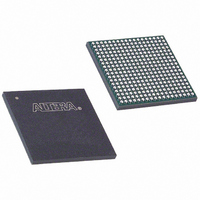
EP3C25F324I7 Altera, EP3C25F324I7 Datasheet - Page 31

EP3C25F324I7
Manufacturer Part Number
EP3C25F324I7
Description
IC CYCLONE III FPGA 25K 324 FBGA
Manufacturer
Altera
Series
Cyclone® IIIr
Datasheets
1.EP3C5F256C8N.pdf
(5 pages)
2.EP3C5F256C8N.pdf
(34 pages)
3.EP3C5F256C8N.pdf
(66 pages)
4.EP3C5F256C8N.pdf
(14 pages)
5.EP3C5F256C8N.pdf
(76 pages)
6.EP3C25F324I7.pdf
(274 pages)
Specifications of EP3C25F324I7
Number Of Logic Elements/cells
24624
Number Of Labs/clbs
1539
Total Ram Bits
608256
Number Of I /o
215
Voltage - Supply
1.15 V ~ 1.25 V
Mounting Type
Surface Mount
Operating Temperature
-40°C ~ 100°C
Package / Case
324-FBGA
Family Name
Cyclone III
Number Of Logic Blocks/elements
24624
# I/os (max)
215
Frequency (max)
437.5MHz
Process Technology
65nm
Operating Supply Voltage (typ)
1.2V
Logic Cells
24624
Ram Bits
608256
Operating Supply Voltage (min)
1.15V
Operating Supply Voltage (max)
1.25V
Operating Temp Range
-40C to 100C
Operating Temperature Classification
Industrial
Mounting
Surface Mount
Pin Count
324
Package Type
FBGA
For Use With
544-2370 - KIT STARTER CYCLONE III EP3C25
Lead Free Status / RoHS Status
Contains lead / RoHS non-compliant
Number Of Gates
-
Lead Free Status / Rohs Status
Not Compliant
Available stocks
Company
Part Number
Manufacturer
Quantity
Price
Company:
Part Number:
EP3C25F324I7N
Manufacturer:
ALTERA32
Quantity:
181
Chapter 2: Logic Elements and Logic Array Blocks in the Cyclone III Device Family
LE Operating Modes
LE Operating Modes
Normal Mode
© December 2009
Altera Corporation
In addition to the three general routing outputs, LEs in a LAB have register chain
outputs, which allows registers in the same LAB to cascade together. The register
chain output allows the LUTs to be used for combinational functions and the registers
to be used for an unrelated shift register implementation. These resources speed up
connections between LABs while saving local interconnect resources.
Cyclone III device family LEs operate in the following modes:
■
■
LE operating modes use LE resources differently. In each mode, there are six available
inputs to the LE. These inputs include the four data inputs from the LAB local
interconnect, the LE carry-in from the previous LE carry-chain, and the register chain
connection. Each input is directed to different destinations to implement the desired
logic function. LAB-wide signals provide clock, asynchronous clear, synchronous
clear, synchronous load, and clock enable control for the register. These LAB-wide
signals are available in all LE modes.
The Quartus
functions, such as counters, adders, subtractors, and arithmetic functions, in
conjunction with parameterized functions such as the library of parameterized
modules (LPM) functions. You can also create special-purpose functions that specify
which LE operating mode to use for optimal performance, if required.
Normal mode is suitable for general logic applications and combinational functions.
In normal mode, four data inputs from the LAB local interconnect are inputs to a
four-input LUT
carry-in (cin) or the data3 signal as one of the inputs to the LUT. LEs in normal
mode support packed registers and register feedback.
Figure 2–2
Figure 2–2. Cyclone III Device Family LEs in Normal Mode
Normal mode
Arithmetic mode
shows LEs in normal mode.
®
II software automatically chooses the appropriate mode for common
data1
data2
data3
cin (from cout
of previous LE)
data4
(Figure
Packed Register Input
2–2). The Quartus II Compiler automatically selects the
Four-Input
LUT
Register Chain
Connection
Register Bypass
clock (LAB Wide)
sload
ena (LAB Wide)
aclr (LAB Wide)
(LAB Wide)
sclear
Register Feedback
(LAB Wide)
D
ENA
CLRN
Q
Cyclone III Device Handbook, Volume 1
Row, Column, and
Direct Link Routing
Local Routing
Row, Column, and
Direct Link Routing
Register
Chain Output
2–3


