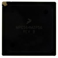
MPC564MZP56 Freescale Semiconductor, MPC564MZP56 Datasheet - Page 101
MPC564MZP56
Manufacturer Part Number
MPC564MZP56
Description
IC MCU 512K FLASH 56MHZ 388-BGA
Manufacturer
Freescale Semiconductor
Series
MPC5xxr
Specifications of MPC564MZP56
Core Processor
PowerPC
Core Size
32-Bit
Speed
56MHz
Connectivity
CAN, EBI/EMI, SCI, SPI, UART/USART
Peripherals
POR, PWM, WDT
Number Of I /o
56
Program Memory Size
512KB (512K x 8)
Program Memory Type
FLASH
Ram Size
32K x 8
Voltage - Supply (vcc/vdd)
2.5 V ~ 2.7 V
Data Converters
A/D 32x10b
Oscillator Type
External
Operating Temperature
-40°C ~ 125°C
Package / Case
388-BGA
Core
PowerPC
Processor Series
MPC5xx
Data Bus Width
32 bit
Maximum Clock Frequency
56 MHz
Data Ram Size
32 KB
On-chip Adc
Yes
Number Of Programmable I/os
56
Number Of Timers
2
Operating Supply Voltage
0 V to 5 V
Mounting Style
SMD/SMT
A/d Bit Size
10 bit
A/d Channels Available
32
Height
1.95 mm
Interface Type
CAN, JTAG, QSPI, SCI, SPI, UART
Length
27 mm
Maximum Operating Temperature
+ 125 C
Minimum Operating Temperature
- 40 C
Supply Voltage (max)
2.7 V, 5.25 V
Supply Voltage (min)
2.5 V, 4.75 V
Width
27 mm
For Use With
MPC564EVB - KIT EVAL FOR MPC561/562/563/564
Lead Free Status / RoHS Status
Contains lead / RoHS non-compliant
Eeprom Size
-
Lead Free Status / Rohs Status
No RoHS Version Available
Available stocks
Company
Part Number
Manufacturer
Quantity
Price
Company:

Part Number:
MPC564MZP56
Manufacturer:
FREESCAL
Quantity:
364
Company:
Part Number:
MPC564MZP56
Manufacturer:
Freescale Semiconductor
Quantity:
10 000
Part Number:
MPC564MZP56
Manufacturer:
FREESCALE
Quantity:
20 000
Company:
Part Number:
MPC564MZP56R2
Manufacturer:
Freescale Semiconductor
Quantity:
10 000


2.2
Table 2-1
Freescale Semiconductor
ADDR[8:31] / SGPIOA[8:31]
DATA[0:31] / SGPIOD[0:31]
TSIZ[0:1]
RD/WR
BURST
BDIP
TS
TA
Signal Name
Signal Summary
describes individual MPC561/MPC563 signals, grouped by functional module.
Signals
No. of
24
32
2
1
1
1
1
1
Table 2-1. MPC561/MPC563 Signal Descriptions
MPC561/MPC563 Reference Manual, Rev. 1.2
Type
I/O
I/O
I/O
I/O
I/O
I/O
I/O
I/O
I/O
I/O
Controlled by
RCW[SC].
See
Controlled by
RCW[SC].
See
TSIZ[0:1]
RD/WR
BURST
BDIP
TS
TA
Function after
Reset
Table
Table
Bus Interface
6-10.
6-10.
1
Address Bus [8:31]. Specifies the physical address of the
bus transaction. The address is driven onto the bus and kept
valid until a transfer acknowledge is received from the slave.
ADDR8 is the MSB for this bus.
Port SGPIOA[8:31]. Allows the signals to be used as
general-purpose inputs/outputs.
Data Bus [0:31]. Provides the general-purpose data path
between the MPC561/MPC563 and all other devices.
Although the data path is a maximum of 32 bits wide, it can
be sized to support 8-, 16-, or 32-bit transfers. DATA0 is the
MSB of the data bus.
Port SGPIOD[0:31]. Allows the signals to be used as
general-purpose inputs/outputs.
Transfer Size [0:1]. Indicates the size of the requested data
transfer in the current bus cycle.
Read/Write. Indicates the direction of the data transfer for a
transaction. A logic one indicates a read from a slave device;
a logic zero indicates a write to a slave device.
Burst Indicator. Driven by the bus master to indicate that the
currently initiated transaction is a burst.
Burst Data In Progress. Indicates to the slave that there is a
data beat following the current data beat.
Transfer Start. Indicates the start of a bus cycle that
transfers data to/from a slave device. This signal is driven by
the master only when it has gained ownership of the bus.
Every master should negate this signal before relinquishing
the bus.
This is an active-low signal and needs an external pull-up
resistor to ensure proper operation and meet signal timing
specifications.
Transfer Acknowledge. This line indicates that the slave
device addressed in the current transaction has accepted
the data transferred by the master (write) or has driven the
data bus with valid data (read). The slave device negates the
TA signal after the end of the transaction. The slave device
will then immediately three-state the TA signal to prevent
contention on the line in case a new transfer that addresses
another slave device(s) is initiated.
This signal is an active-low signal and needs an external
pull-up resistor to ensure proper operation and conform to
signal timing specifications.
Description
Signal Descriptions
2-3
Related parts for MPC564MZP56
Image
Part Number
Description
Manufacturer
Datasheet
Request
R

Part Number:
Description:
MPC5 1K0 5%
Manufacturer:
TE Connectivity
Datasheet:


Part Number:
Description:
MPC5 500R 5%
Manufacturer:
TE Connectivity
Datasheet:

Part Number:
Description:
MPC5 5K0 5%
Manufacturer:
Tyco Electronics
Datasheet:
Part Number:
Description:
MPC5 5R0 5%
Manufacturer:
Tyco Electronics
Datasheet:
Part Number:
Description:
MPC5 50K 5%
Manufacturer:
Tyco Electronics
Datasheet:
Part Number:
Description:
MPC5 1R0 5%
Manufacturer:
Tyco Electronics
Datasheet:

Part Number:
Description:
Manufacturer:
Freescale Semiconductor, Inc
Datasheet:
Part Number:
Description:
Manufacturer:
Freescale Semiconductor, Inc
Datasheet:
Part Number:
Description:
Manufacturer:
Freescale Semiconductor, Inc
Datasheet:
Part Number:
Description:
Manufacturer:
Freescale Semiconductor, Inc
Datasheet:
Part Number:
Description:
Manufacturer:
Freescale Semiconductor, Inc
Datasheet: