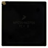
MPC564MZP56 Freescale Semiconductor, MPC564MZP56 Datasheet - Page 1085

MPC564MZP56
Manufacturer Part Number
MPC564MZP56
Description
IC MCU 512K FLASH 56MHZ 388-BGA
Manufacturer
Freescale Semiconductor
Series
MPC5xxr
Specifications of MPC564MZP56
Core Processor
PowerPC
Core Size
32-Bit
Speed
56MHz
Connectivity
CAN, EBI/EMI, SCI, SPI, UART/USART
Peripherals
POR, PWM, WDT
Number Of I /o
56
Program Memory Size
512KB (512K x 8)
Program Memory Type
FLASH
Ram Size
32K x 8
Voltage - Supply (vcc/vdd)
2.5 V ~ 2.7 V
Data Converters
A/D 32x10b
Oscillator Type
External
Operating Temperature
-40°C ~ 125°C
Package / Case
388-BGA
Core
PowerPC
Processor Series
MPC5xx
Data Bus Width
32 bit
Maximum Clock Frequency
56 MHz
Data Ram Size
32 KB
On-chip Adc
Yes
Number Of Programmable I/os
56
Number Of Timers
2
Operating Supply Voltage
0 V to 5 V
Mounting Style
SMD/SMT
A/d Bit Size
10 bit
A/d Channels Available
32
Height
1.95 mm
Interface Type
CAN, JTAG, QSPI, SCI, SPI, UART
Length
27 mm
Maximum Operating Temperature
+ 125 C
Minimum Operating Temperature
- 40 C
Supply Voltage (max)
2.7 V, 5.25 V
Supply Voltage (min)
2.5 V, 4.75 V
Width
27 mm
For Use With
MPC564EVB - KIT EVAL FOR MPC561/562/563/564
Lead Free Status / RoHS Status
Contains lead / RoHS non-compliant
Eeprom Size
-
Lead Free Status / Rohs Status
No RoHS Version Available
Available stocks
Company
Part Number
Manufacturer
Quantity
Price
Company:
Part Number:
MPC564MZP56
Manufacturer:
FREESCAL
Quantity:
364
Company:
Part Number:
MPC564MZP56
Manufacturer:
Freescale Semiconductor
Quantity:
10 000
Part Number:
MPC564MZP56
Manufacturer:
FREESCALE
Quantity:
20 000
Company:
Part Number:
MPC564MZP56R2
Manufacturer:
Freescale Semiconductor
Quantity:
10 000
- Current page: 1085 of 1420
- Download datasheet (11Mb)
During the capture-IR controller state, the parallel inputs to the instruction shift register are loaded with
the CLAMP command code.
25.1.3.1
The external test (EXTEST) instruction selects the 520-bit boundary scan register. EXTEST also asserts
internal reset for the MPC561/MPC563 system logic to force a predictable beginning internal state while
performing external boundary scan operations.
By using the TAP, the register is capable of:
25.1.3.2
The SAMPLE/PRELOAD instruction initializes the boundary scan register output cells prior to selection
of EXTEST. This initialization ensures that known data will appear on the outputs when entering the
EXTEST instruction. The SAMPLE/PRELOAD instruction also provides a means to obtain a snapshot of
system data and control signals.
25.1.3.3
The BYPASS instruction selects the single-bit bypass register as shown in
register path from TDI to the bypass register and, finally, to TDO, circumventing the 520-bit boundary
scan register. This instruction is used to enhance test efficiency when a component other than the
MPC561/MPC563 becomes the device under test.
When the bypass register is selected by the current instruction, the shift register stage is set to a logic zero
on the rising edge of TCK in the capture-DR controller state. Therefore, the first bit to be shifted out after
selecting the bypass register will always be a logic zero.
Freescale Semiconductor
a) scanning user-defined values into the output buffers
b) capturing values presented to input pins
c) controlling the output drive of three-state output or bidirectional pins
EXTEST
SAMPLE/PRELOAD
BYPASS
Since there is no internal synchronization between the scan chain clock
(TCK) and the system clock (CLKOUT), there must be provision of some
form of external synchronization to achieve meaningful results.
FROM TDI
SHIFT DR
0
MPC561/MPC563 Reference Manual, Rev. 1.2
Figure 25-5. Bypass Register
G1
1
1
Mux
NOTE
CLOCK DR
D
C
Figure
IEEE 1149.1-Compliant Interface (JTAG)
TO TDO
25-5. This creates a shift
25-31
Related parts for MPC564MZP56
Image
Part Number
Description
Manufacturer
Datasheet
Request
R

Part Number:
Description:
MPC5 1K0 5%
Manufacturer:
TE Connectivity
Datasheet:

Part Number:
Description:
MPC5 500R 5%
Manufacturer:
TE Connectivity
Datasheet:

Part Number:
Description:
MPC5 5K0 5%
Manufacturer:
Tyco Electronics
Datasheet:

Part Number:
Description:
MPC5 5R0 5%
Manufacturer:
Tyco Electronics
Datasheet:

Part Number:
Description:
MPC5 50K 5%
Manufacturer:
Tyco Electronics
Datasheet:

Part Number:
Description:
MPC5 1R0 5%
Manufacturer:
Tyco Electronics
Datasheet:
Part Number:
Description:
Manufacturer:
Freescale Semiconductor, Inc
Datasheet:
Part Number:
Description:
Manufacturer:
Freescale Semiconductor, Inc
Datasheet:
Part Number:
Description:
Manufacturer:
Freescale Semiconductor, Inc
Datasheet:
Part Number:
Description:
Manufacturer:
Freescale Semiconductor, Inc
Datasheet:
Part Number:
Description:
Manufacturer:
Freescale Semiconductor, Inc
Datasheet:


