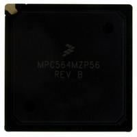
MPC564MZP56 Freescale Semiconductor, MPC564MZP56 Datasheet - Page 985

MPC564MZP56
Manufacturer Part Number
MPC564MZP56
Description
IC MCU 512K FLASH 56MHZ 388-BGA
Manufacturer
Freescale Semiconductor
Series
MPC5xxr
Specifications of MPC564MZP56
Core Processor
PowerPC
Core Size
32-Bit
Speed
56MHz
Connectivity
CAN, EBI/EMI, SCI, SPI, UART/USART
Peripherals
POR, PWM, WDT
Number Of I /o
56
Program Memory Size
512KB (512K x 8)
Program Memory Type
FLASH
Ram Size
32K x 8
Voltage - Supply (vcc/vdd)
2.5 V ~ 2.7 V
Data Converters
A/D 32x10b
Oscillator Type
External
Operating Temperature
-40°C ~ 125°C
Package / Case
388-BGA
Core
PowerPC
Processor Series
MPC5xx
Data Bus Width
32 bit
Maximum Clock Frequency
56 MHz
Data Ram Size
32 KB
On-chip Adc
Yes
Number Of Programmable I/os
56
Number Of Timers
2
Operating Supply Voltage
0 V to 5 V
Mounting Style
SMD/SMT
A/d Bit Size
10 bit
A/d Channels Available
32
Height
1.95 mm
Interface Type
CAN, JTAG, QSPI, SCI, SPI, UART
Length
27 mm
Maximum Operating Temperature
+ 125 C
Minimum Operating Temperature
- 40 C
Supply Voltage (max)
2.7 V, 5.25 V
Supply Voltage (min)
2.5 V, 4.75 V
Width
27 mm
For Use With
MPC564EVB - KIT EVAL FOR MPC561/562/563/564
Lead Free Status / RoHS Status
Contains lead / RoHS non-compliant
Eeprom Size
-
Lead Free Status / Rohs Status
No RoHS Version Available
Available stocks
Company
Part Number
Manufacturer
Quantity
Price
Company:
Part Number:
MPC564MZP56
Manufacturer:
FREESCAL
Quantity:
364
Company:
Part Number:
MPC564MZP56
Manufacturer:
Freescale Semiconductor
Quantity:
10 000
Part Number:
MPC564MZP56
Manufacturer:
FREESCALE
Quantity:
20 000
Company:
Part Number:
MPC564MZP56R2
Manufacturer:
Freescale Semiconductor
Quantity:
10 000
- Current page: 985 of 1420
- Download datasheet (11Mb)
24.6.1.9
The DTA1 and DTA2 registers allow data trace messaging (DTM) to be restricted to reads, writes or both
for a user programmable address range. Two DTA registers allow two address ranges to be selected for
DTM. Refer to
Freescale Semiconductor
.
RCPU
Bits
0:22
RSTI
RSTI
RSTI
Field
Field
Field
Addr
16 bit
32 bit
8 bit
MSB
Nexus
47
31
15
47:25
Data Trace Attributes 1 and 2 Registers (DTA1 and DTA2)
Bits
The RWD field of the UDI register is shared with the WD field of the RWA
register.
Table 24-15
46
30
14
MS Byte
DTEA
Name
Reserved – Read as Zeros
Figure 24-10. READI Data Trace Attributes 1 Register (DTA1)
45
29
13
1
for register bit descriptions.
DTEA
READI Data Trace Attributes 2 Register (DTA2)
44
28
12
The Read/Write End Field defines the end address for the address range. Refer to
Table
Table 24-15. DTA 1 AND 2 Bit Descriptions
Reserved – Read as Zeros
MPC561/MPC563 Reference Manual, Rev. 1.2
Figure 24-9. RWD Field Configuration
43
27
11
24-16.
42
26
10
0000_0000_0000_00
0x14 (DTA1), 0x15 (DTA2)
0000_0000_0000_0000
0000_0000_0000_0000
41
25
9
DTSA
NOTE
40
24
8
DTEA
39
23
7
MS Byte
Description
38
22
6
37
21
5
DTSA
36
20
4
LS Byte
LS Byte
LS Byte
35
19
3
34
18
2
ERR
ERR
ERR
33
17
1
READI Module
TA
00
LSB
DV
DV
DV
LSB
32
16
0
24-17
Related parts for MPC564MZP56
Image
Part Number
Description
Manufacturer
Datasheet
Request
R

Part Number:
Description:
MPC5 1K0 5%
Manufacturer:
TE Connectivity
Datasheet:

Part Number:
Description:
MPC5 500R 5%
Manufacturer:
TE Connectivity
Datasheet:

Part Number:
Description:
MPC5 5K0 5%
Manufacturer:
Tyco Electronics
Datasheet:

Part Number:
Description:
MPC5 5R0 5%
Manufacturer:
Tyco Electronics
Datasheet:

Part Number:
Description:
MPC5 50K 5%
Manufacturer:
Tyco Electronics
Datasheet:

Part Number:
Description:
MPC5 1R0 5%
Manufacturer:
Tyco Electronics
Datasheet:
Part Number:
Description:
Manufacturer:
Freescale Semiconductor, Inc
Datasheet:
Part Number:
Description:
Manufacturer:
Freescale Semiconductor, Inc
Datasheet:
Part Number:
Description:
Manufacturer:
Freescale Semiconductor, Inc
Datasheet:
Part Number:
Description:
Manufacturer:
Freescale Semiconductor, Inc
Datasheet:
Part Number:
Description:
Manufacturer:
Freescale Semiconductor, Inc
Datasheet:


