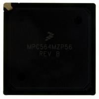
MPC564MZP56 Freescale Semiconductor, MPC564MZP56 Datasheet - Page 722

MPC564MZP56
Manufacturer Part Number
MPC564MZP56
Description
IC MCU 512K FLASH 56MHZ 388-BGA
Manufacturer
Freescale Semiconductor
Series
MPC5xxr
Specifications of MPC564MZP56
Core Processor
PowerPC
Core Size
32-Bit
Speed
56MHz
Connectivity
CAN, EBI/EMI, SCI, SPI, UART/USART
Peripherals
POR, PWM, WDT
Number Of I /o
56
Program Memory Size
512KB (512K x 8)
Program Memory Type
FLASH
Ram Size
32K x 8
Voltage - Supply (vcc/vdd)
2.5 V ~ 2.7 V
Data Converters
A/D 32x10b
Oscillator Type
External
Operating Temperature
-40°C ~ 125°C
Package / Case
388-BGA
Core
PowerPC
Processor Series
MPC5xx
Data Bus Width
32 bit
Maximum Clock Frequency
56 MHz
Data Ram Size
32 KB
On-chip Adc
Yes
Number Of Programmable I/os
56
Number Of Timers
2
Operating Supply Voltage
0 V to 5 V
Mounting Style
SMD/SMT
A/d Bit Size
10 bit
A/d Channels Available
32
Height
1.95 mm
Interface Type
CAN, JTAG, QSPI, SCI, SPI, UART
Length
27 mm
Maximum Operating Temperature
+ 125 C
Minimum Operating Temperature
- 40 C
Supply Voltage (max)
2.7 V, 5.25 V
Supply Voltage (min)
2.5 V, 4.75 V
Width
27 mm
For Use With
MPC564EVB - KIT EVAL FOR MPC561/562/563/564
Lead Free Status / RoHS Status
Contains lead / RoHS non-compliant
Eeprom Size
-
Lead Free Status / Rohs Status
No RoHS Version Available
Available stocks
Company
Part Number
Manufacturer
Quantity
Price
Company:
Part Number:
MPC564MZP56
Manufacturer:
FREESCAL
Quantity:
364
Company:
Part Number:
MPC564MZP56
Manufacturer:
Freescale Semiconductor
Quantity:
10 000
Part Number:
MPC564MZP56
Manufacturer:
FREESCALE
Quantity:
20 000
Company:
Part Number:
MPC564MZP56R2
Manufacturer:
Freescale Semiconductor
Quantity:
10 000
- Current page: 722 of 1420
- Download datasheet (11Mb)
CAN 2.0B Controller Module
16.7.5
16-28
SRESET
CNRX0
Signal
Bits
8:15
2:3
4:5
6:7
0
1
Field
Addr
Control Register 1 (CANCTRL1)
1
2
CANCTRL1
MSB
BOFFMSK
TXMODE[1:0]
RXMODE
ERRMSK
TXMODE
Full CMOS drive indicates that both dominant and recessive levels are driven by the chip.
Open drain drive indicates that only a dominant level is driven by the chip. During a recessive
level, the CNTX0 signal is disabled (three stated), and the electrical level is achieved by external
pull-up/pull-down devices. The assertion of both Tx mode bits causes the polarity inversion to be
cancelled (open drain mode forces the polarity to be positive).
0
RX1
Name
X
X
—
1X
00
01
1
0x30 7086 (CANCTRL1_A); 0x30 7486 (CANCTRL1_B); 0x30 7886 (CANCTRL1_C)
RX0
0
1
2
Bus off interrupt mask. The BOFF MASK bit provides a mask for the bus off interrupt.
0 Bus off interrupt disabled
1 Bus off interrupt enabled
Error interrupt mask. The ERRMSK bit provides a mask for the error interrupt.
0 Error interrupt disabled
1 Error interrupt enabled
Reserved
Receive signal configuration control. These bits control the configuration of the CNRX0
signals. Refer to
Transmit signal configuration control. This bit field controls the configuration of the CNTX0
signals. Refer to
See
CANCTRL0
Full CMOS
Full CMOS
Open drain
3
0 CNRX0 signal is interpreted as a dominant bit
1 CNRX0 signal is interpreted as a recessive bit
0 CNRX0 signal is interpreted as a recessive bit
1 CNRX0 signal is interpreted as a dominant bit
Table 16-16
Figure 16-12. Control Register 1 (CANCTRL1)
Table 16-15. Transmit Signal Configuration
Table 16-14. Rx MODE[1:0] Configuration
Table 16-13. CANCTRL0 Bit Descriptions
MPC561/MPC563 Reference Manual, Rev. 1.2
4
1
1
2
5
; positive polarity (CNTX0 = 0 is a dominant level)
; negative polarity (CNTX0 = 1 is a dominant level)
; positive polarity
Table
Table
and
6
Section 16.7.5, “Control Register 1
16-14.
16-15.
0000_0000_0000_0000
TransmitSignal Configuration
7
SAMP
Receive Signal Configuration
8
Description
—
9
TSYNC LBUF
10
(CANCTRL1).”
11
—
12
Freescale Semiconductor
13
PROPSEG
14
LSB
15
Related parts for MPC564MZP56
Image
Part Number
Description
Manufacturer
Datasheet
Request
R

Part Number:
Description:
MPC5 1K0 5%
Manufacturer:
TE Connectivity
Datasheet:

Part Number:
Description:
MPC5 500R 5%
Manufacturer:
TE Connectivity
Datasheet:

Part Number:
Description:
MPC5 5K0 5%
Manufacturer:
Tyco Electronics
Datasheet:

Part Number:
Description:
MPC5 5R0 5%
Manufacturer:
Tyco Electronics
Datasheet:

Part Number:
Description:
MPC5 50K 5%
Manufacturer:
Tyco Electronics
Datasheet:

Part Number:
Description:
MPC5 1R0 5%
Manufacturer:
Tyco Electronics
Datasheet:
Part Number:
Description:
Manufacturer:
Freescale Semiconductor, Inc
Datasheet:
Part Number:
Description:
Manufacturer:
Freescale Semiconductor, Inc
Datasheet:
Part Number:
Description:
Manufacturer:
Freescale Semiconductor, Inc
Datasheet:
Part Number:
Description:
Manufacturer:
Freescale Semiconductor, Inc
Datasheet:
Part Number:
Description:
Manufacturer:
Freescale Semiconductor, Inc
Datasheet:


