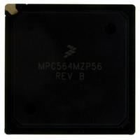
MPC564MZP56 Freescale Semiconductor, MPC564MZP56 Datasheet - Page 808

MPC564MZP56
Manufacturer Part Number
MPC564MZP56
Description
IC MCU 512K FLASH 56MHZ 388-BGA
Manufacturer
Freescale Semiconductor
Series
MPC5xxr
Specifications of MPC564MZP56
Core Processor
PowerPC
Core Size
32-Bit
Speed
56MHz
Connectivity
CAN, EBI/EMI, SCI, SPI, UART/USART
Peripherals
POR, PWM, WDT
Number Of I /o
56
Program Memory Size
512KB (512K x 8)
Program Memory Type
FLASH
Ram Size
32K x 8
Voltage - Supply (vcc/vdd)
2.5 V ~ 2.7 V
Data Converters
A/D 32x10b
Oscillator Type
External
Operating Temperature
-40°C ~ 125°C
Package / Case
388-BGA
Core
PowerPC
Processor Series
MPC5xx
Data Bus Width
32 bit
Maximum Clock Frequency
56 MHz
Data Ram Size
32 KB
On-chip Adc
Yes
Number Of Programmable I/os
56
Number Of Timers
2
Operating Supply Voltage
0 V to 5 V
Mounting Style
SMD/SMT
A/d Bit Size
10 bit
A/d Channels Available
32
Height
1.95 mm
Interface Type
CAN, JTAG, QSPI, SCI, SPI, UART
Length
27 mm
Maximum Operating Temperature
+ 125 C
Minimum Operating Temperature
- 40 C
Supply Voltage (max)
2.7 V, 5.25 V
Supply Voltage (min)
2.5 V, 4.75 V
Width
27 mm
For Use With
MPC564EVB - KIT EVAL FOR MPC561/562/563/564
Lead Free Status / RoHS Status
Contains lead / RoHS non-compliant
Eeprom Size
-
Lead Free Status / Rohs Status
No RoHS Version Available
Available stocks
Company
Part Number
Manufacturer
Quantity
Price
Company:
Part Number:
MPC564MZP56
Manufacturer:
FREESCAL
Quantity:
364
Company:
Part Number:
MPC564MZP56
Manufacturer:
Freescale Semiconductor
Quantity:
10 000
Part Number:
MPC564MZP56
Manufacturer:
FREESCALE
Quantity:
20 000
Company:
Part Number:
MPC564MZP56R2
Manufacturer:
Freescale Semiconductor
Quantity:
10 000
- Current page: 808 of 1420
- Download datasheet (11Mb)
Peripheral Pin Multiplexing (PPM) Module
18.2
The PPM occupies 100 bytes of address space, arranged as 50 16-bit entries. All registers must be read or
written through half-word (16-bit) accesses. Reserved register addresses return zeros when read and
cannot be written to.
18-2
Access
— A_T2CLK to B_T2CLK
S/U
S/U
S
S
S
S
S
T
—
—
—
—
1
2
1
1
1
1
Programming Model
3
3
MPC555
Register Name
TX_CONFIG_1
TX_CONFIG_2
RX_CONFIG_1
RX_CONFIG_2
Parallel TX/RX Protocol
Table 18-1
PPMMCR
RX_DATA
PPMTCR
PPMPCR
Reserved
Reserved
Reserved
Reserved
N=31
Figure 18-1. N-Signal I/O Compared with PPM I/O
0
1
N data signals
shows the memory map for the PPM module.
MPC561/MPC563 Reference Manual, Rev. 1.2
External
Device
Table 18-1. PPM Memory Map
0x30 5C0A
0x30 5C0C
0x30 5C0E
0x30 5C00
0x30 5C02
0x30 5C04
0x30 5C06
0x30 5C08
0x30 5C10
0x30 5C12
0x30 5C14
0x30 5C16
0x30 5C18
Address
—
Receives data from RX_SHIFTER on SAMP[0:2] update rate
MPC563
MPC561/
PPM TX/RX Protocol
Module Configuration Register
Test Configuration Register
TX Output Configuration
TX Output Configuration
RX Input Configuration
RX Input Configuration
6 signals (maximum 4 data signals)
PPM Control Register
TSYNC
TCLK
TX1
TX0
RX1
RX0
Usage
—
—
—
—
External
Device
Freescale Semiconductor
Related parts for MPC564MZP56
Image
Part Number
Description
Manufacturer
Datasheet
Request
R

Part Number:
Description:
MPC5 1K0 5%
Manufacturer:
TE Connectivity
Datasheet:

Part Number:
Description:
MPC5 500R 5%
Manufacturer:
TE Connectivity
Datasheet:

Part Number:
Description:
MPC5 5K0 5%
Manufacturer:
Tyco Electronics
Datasheet:

Part Number:
Description:
MPC5 5R0 5%
Manufacturer:
Tyco Electronics
Datasheet:

Part Number:
Description:
MPC5 50K 5%
Manufacturer:
Tyco Electronics
Datasheet:

Part Number:
Description:
MPC5 1R0 5%
Manufacturer:
Tyco Electronics
Datasheet:
Part Number:
Description:
Manufacturer:
Freescale Semiconductor, Inc
Datasheet:
Part Number:
Description:
Manufacturer:
Freescale Semiconductor, Inc
Datasheet:
Part Number:
Description:
Manufacturer:
Freescale Semiconductor, Inc
Datasheet:
Part Number:
Description:
Manufacturer:
Freescale Semiconductor, Inc
Datasheet:
Part Number:
Description:
Manufacturer:
Freescale Semiconductor, Inc
Datasheet:


