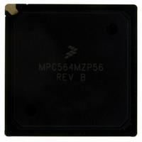
MPC564MZP56 Freescale Semiconductor, MPC564MZP56 Datasheet - Page 412

MPC564MZP56
Manufacturer Part Number
MPC564MZP56
Description
IC MCU 512K FLASH 56MHZ 388-BGA
Manufacturer
Freescale Semiconductor
Series
MPC5xxr
Specifications of MPC564MZP56
Core Processor
PowerPC
Core Size
32-Bit
Speed
56MHz
Connectivity
CAN, EBI/EMI, SCI, SPI, UART/USART
Peripherals
POR, PWM, WDT
Number Of I /o
56
Program Memory Size
512KB (512K x 8)
Program Memory Type
FLASH
Ram Size
32K x 8
Voltage - Supply (vcc/vdd)
2.5 V ~ 2.7 V
Data Converters
A/D 32x10b
Oscillator Type
External
Operating Temperature
-40°C ~ 125°C
Package / Case
388-BGA
Core
PowerPC
Processor Series
MPC5xx
Data Bus Width
32 bit
Maximum Clock Frequency
56 MHz
Data Ram Size
32 KB
On-chip Adc
Yes
Number Of Programmable I/os
56
Number Of Timers
2
Operating Supply Voltage
0 V to 5 V
Mounting Style
SMD/SMT
A/d Bit Size
10 bit
A/d Channels Available
32
Height
1.95 mm
Interface Type
CAN, JTAG, QSPI, SCI, SPI, UART
Length
27 mm
Maximum Operating Temperature
+ 125 C
Minimum Operating Temperature
- 40 C
Supply Voltage (max)
2.7 V, 5.25 V
Supply Voltage (min)
2.5 V, 4.75 V
Width
27 mm
For Use With
MPC564EVB - KIT EVAL FOR MPC561/562/563/564
Lead Free Status / RoHS Status
Contains lead / RoHS non-compliant
Eeprom Size
-
Lead Free Status / Rohs Status
No RoHS Version Available
Available stocks
Company
Part Number
Manufacturer
Quantity
Price
Company:
Part Number:
MPC564MZP56
Manufacturer:
FREESCAL
Quantity:
364
Company:
Part Number:
MPC564MZP56
Manufacturer:
Freescale Semiconductor
Quantity:
10 000
Part Number:
MPC564MZP56
Manufacturer:
FREESCALE
Quantity:
20 000
Company:
Part Number:
MPC564MZP56R2
Manufacturer:
Freescale Semiconductor
Quantity:
10 000
- Current page: 412 of 1420
- Download datasheet (11Mb)
Memory Controller
The CSx timing is defined by the setup time required between the address lines and the CE line. The
memory controller allows specification of the CS timing to meet the setup time required by the peripheral
device. This is accomplished through the ACS field in the base register. In
set to 0b11, so CSx is asserted half a clock cycle after the address lines are valid.
10.3.3
The TRLX field is provided for memory systems that need a more relaxed timing between signals. When
TRLX is set and ACS = 0b00, the memory controller inserts an additional cycle between address and
strobes (CS line and WE/OE).
When TRLX and CSNT are both set in a write to memory, the strobe lines (WE/BE[0:3] and CS, if ACS
= 0b00) are negated one clock earlier than in the regular case.
Figure 10-11
10-14
•
•
Strobes (OE and CS) assertion time is delayed one clock relative to address (TRLX bit set effect).
Strobe (CS) is further delayed (half-clock) relative to address due to ACS field being set to 11.
Relaxed Timing Examples
Address
shows a read access with relaxed timing. Note the following:
CLOCK
RD/WR
In the case of a bank selected to work with external transfer acknowledge
(SETA = 1) and TRLX = 1, the memory controller does not support external
devices that provide TA to complete the transfer with zero wait states. The
minimum access duration in this case equals three clock cycles.
Data
CS
TS
TA
Figure 10-10. Peripheral Devices Basic Timing (ACS = 11, TRLX = 0)
MPC561/MPC563 Reference Manual, Rev. 1.2
NOTE
ACS = 11
Figure
10-10, the ACS bits are
CSNT = 1
Freescale Semiconductor
Related parts for MPC564MZP56
Image
Part Number
Description
Manufacturer
Datasheet
Request
R

Part Number:
Description:
MPC5 1K0 5%
Manufacturer:
TE Connectivity
Datasheet:

Part Number:
Description:
MPC5 500R 5%
Manufacturer:
TE Connectivity
Datasheet:

Part Number:
Description:
MPC5 5K0 5%
Manufacturer:
Tyco Electronics
Datasheet:

Part Number:
Description:
MPC5 5R0 5%
Manufacturer:
Tyco Electronics
Datasheet:

Part Number:
Description:
MPC5 50K 5%
Manufacturer:
Tyco Electronics
Datasheet:

Part Number:
Description:
MPC5 1R0 5%
Manufacturer:
Tyco Electronics
Datasheet:
Part Number:
Description:
Manufacturer:
Freescale Semiconductor, Inc
Datasheet:
Part Number:
Description:
Manufacturer:
Freescale Semiconductor, Inc
Datasheet:
Part Number:
Description:
Manufacturer:
Freescale Semiconductor, Inc
Datasheet:
Part Number:
Description:
Manufacturer:
Freescale Semiconductor, Inc
Datasheet:
Part Number:
Description:
Manufacturer:
Freescale Semiconductor, Inc
Datasheet:


