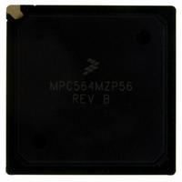
MPC564MZP56 Freescale Semiconductor, MPC564MZP56 Datasheet - Page 1099

MPC564MZP56
Manufacturer Part Number
MPC564MZP56
Description
IC MCU 512K FLASH 56MHZ 388-BGA
Manufacturer
Freescale Semiconductor
Series
MPC5xxr
Specifications of MPC564MZP56
Core Processor
PowerPC
Core Size
32-Bit
Speed
56MHz
Connectivity
CAN, EBI/EMI, SCI, SPI, UART/USART
Peripherals
POR, PWM, WDT
Number Of I /o
56
Program Memory Size
512KB (512K x 8)
Program Memory Type
FLASH
Ram Size
32K x 8
Voltage - Supply (vcc/vdd)
2.5 V ~ 2.7 V
Data Converters
A/D 32x10b
Oscillator Type
External
Operating Temperature
-40°C ~ 125°C
Package / Case
388-BGA
Core
PowerPC
Processor Series
MPC5xx
Data Bus Width
32 bit
Maximum Clock Frequency
56 MHz
Data Ram Size
32 KB
On-chip Adc
Yes
Number Of Programmable I/os
56
Number Of Timers
2
Operating Supply Voltage
0 V to 5 V
Mounting Style
SMD/SMT
A/d Bit Size
10 bit
A/d Channels Available
32
Height
1.95 mm
Interface Type
CAN, JTAG, QSPI, SCI, SPI, UART
Length
27 mm
Maximum Operating Temperature
+ 125 C
Minimum Operating Temperature
- 40 C
Supply Voltage (max)
2.7 V, 5.25 V
Supply Voltage (min)
2.5 V, 4.75 V
Width
27 mm
For Use With
MPC564EVB - KIT EVAL FOR MPC561/562/563/564
Lead Free Status / RoHS Status
Contains lead / RoHS non-compliant
Eeprom Size
-
Lead Free Status / Rohs Status
No RoHS Version Available
Available stocks
Company
Part Number
Manufacturer
Quantity
Price
Company:
Part Number:
MPC564MZP56
Manufacturer:
FREESCAL
Quantity:
364
Company:
Part Number:
MPC564MZP56
Manufacturer:
Freescale Semiconductor
Quantity:
10 000
Part Number:
MPC564MZP56
Manufacturer:
FREESCALE
Quantity:
20 000
Company:
Part Number:
MPC564MZP56R2
Manufacturer:
Freescale Semiconductor
Quantity:
10 000
- Current page: 1099 of 1420
- Download datasheet (11Mb)
A.2.9.5
This MPC562/MPC564 instruction is divided into two segments. The left segment is either fully bypassed
by a 16-bit field or by a shorter field which is decompressed according to fixed rules. The right segment
is compressed and mapped into a vocabulary. The vocabulary location is programmable. The compressed
fields must be swapped in the compressed instruction order to follow the rule that bypass appears only in
the second field of a compressed instruction.
The definition of the class includes:
When the vocabulary is located in RAM #1, the class is referred to as CLASS_4band when the vocabulary
is located in RAM #2, the class is referred to as CLASS_4a. Refer to
A.2.10
Table A-4
The un-compressed instruction of two half-words are referred as H1 & H2. The compressed instruction
can be built out of: (1) X1 field – representing a vocabulary pointer for encoding of either H1 or H1+H2;
(2) X2 field – representing a vocabulary pointer for encoding of H2; and (3) BP – representing a bypass
field.
Vocabularies V1 and V2 refer to the 16 MSB and 16 LSB of the uncompressed instruction, respectively.
A.2.11
The compression process is implemented by the following steps. See
Freescale Semiconductor
.
MSB
•
•
•
•
•
•
•
•
•
16-bit segment #1 – to be bypassed
4-bit class
TP1 length=2-9
TP2 length=0xB, 0xC, 0xD, or 0xE indicating a 0, 10, 15 or 16 bit bypass, respectively.
TP1 base address = base address of segment #1 vocabulary in RAM #1, if it exists there
TP2 base address = base address of segment #1 vocabulary in RAM #2, if it exists there
DS=1
AS=0 or 1 directing access to the vocabulary in RAM #1 or RAM #2, respectively.
User code compilation/linking
Vocabulary and class generation
User application code compression by a software compression tool
summarizes the programming for all possible compressed instruction layouts.
Instruction Layout Programming Summary
Compression Process
Left Segment Bypass and Right Segment Compression—CLASS_4
2- to 9-bit TP1 for segment #2
Figure A-10. CLASS_4 Instruction Layout
MPC561/MPC563 Reference Manual, Rev. 1.2
Uncompressed Instruction
Compressed Instruction
16-bit segment #2 – to be compressed
0-, 10-, 15- or 16-bit bypass for segment #1
Table
Figure
MPC562/MPC564 Compression Features
A-4.
A-11.
A-11
Related parts for MPC564MZP56
Image
Part Number
Description
Manufacturer
Datasheet
Request
R

Part Number:
Description:
MPC5 1K0 5%
Manufacturer:
TE Connectivity
Datasheet:

Part Number:
Description:
MPC5 500R 5%
Manufacturer:
TE Connectivity
Datasheet:

Part Number:
Description:
MPC5 5K0 5%
Manufacturer:
Tyco Electronics
Datasheet:

Part Number:
Description:
MPC5 5R0 5%
Manufacturer:
Tyco Electronics
Datasheet:

Part Number:
Description:
MPC5 50K 5%
Manufacturer:
Tyco Electronics
Datasheet:

Part Number:
Description:
MPC5 1R0 5%
Manufacturer:
Tyco Electronics
Datasheet:
Part Number:
Description:
Manufacturer:
Freescale Semiconductor, Inc
Datasheet:
Part Number:
Description:
Manufacturer:
Freescale Semiconductor, Inc
Datasheet:
Part Number:
Description:
Manufacturer:
Freescale Semiconductor, Inc
Datasheet:
Part Number:
Description:
Manufacturer:
Freescale Semiconductor, Inc
Datasheet:
Part Number:
Description:
Manufacturer:
Freescale Semiconductor, Inc
Datasheet:


