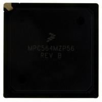
MPC564MZP56 Freescale Semiconductor, MPC564MZP56 Datasheet - Page 500

MPC564MZP56
Manufacturer Part Number
MPC564MZP56
Description
IC MCU 512K FLASH 56MHZ 388-BGA
Manufacturer
Freescale Semiconductor
Series
MPC5xxr
Specifications of MPC564MZP56
Core Processor
PowerPC
Core Size
32-Bit
Speed
56MHz
Connectivity
CAN, EBI/EMI, SCI, SPI, UART/USART
Peripherals
POR, PWM, WDT
Number Of I /o
56
Program Memory Size
512KB (512K x 8)
Program Memory Type
FLASH
Ram Size
32K x 8
Voltage - Supply (vcc/vdd)
2.5 V ~ 2.7 V
Data Converters
A/D 32x10b
Oscillator Type
External
Operating Temperature
-40°C ~ 125°C
Package / Case
388-BGA
Core
PowerPC
Processor Series
MPC5xx
Data Bus Width
32 bit
Maximum Clock Frequency
56 MHz
Data Ram Size
32 KB
On-chip Adc
Yes
Number Of Programmable I/os
56
Number Of Timers
2
Operating Supply Voltage
0 V to 5 V
Mounting Style
SMD/SMT
A/d Bit Size
10 bit
A/d Channels Available
32
Height
1.95 mm
Interface Type
CAN, JTAG, QSPI, SCI, SPI, UART
Length
27 mm
Maximum Operating Temperature
+ 125 C
Minimum Operating Temperature
- 40 C
Supply Voltage (max)
2.7 V, 5.25 V
Supply Voltage (min)
2.5 V, 4.75 V
Width
27 mm
For Use With
MPC564EVB - KIT EVAL FOR MPC561/562/563/564
Lead Free Status / RoHS Status
Contains lead / RoHS non-compliant
Eeprom Size
-
Lead Free Status / Rohs Status
No RoHS Version Available
Available stocks
Company
Part Number
Manufacturer
Quantity
Price
Company:
Part Number:
MPC564MZP56
Manufacturer:
FREESCAL
Quantity:
364
Company:
Part Number:
MPC564MZP56
Manufacturer:
Freescale Semiconductor
Quantity:
10 000
Part Number:
MPC564MZP56
Manufacturer:
FREESCALE
Quantity:
20 000
Company:
Part Number:
MPC564MZP56R2
Manufacturer:
Freescale Semiconductor
Quantity:
10 000
- Current page: 500 of 1420
- Download datasheet (11Mb)
QADC64E Legacy Mode Operation
13.4.2
The internal multiplexer selects one of the 16 analog input signals for conversion. The selected input is
connected to the sample buffer amplifier. The multiplexer also includes positive and negative stress
protection circuitry, which prevents deselected channels from affecting the selected channel when current
is injected into the deselected channels. Refer to
current levels.
13.4.3
The sample buffer is used to raise the effective input impedance of the A/D converter, so that external
components (higher bandwidth or higher impedance) are less critical to accuracy. The input voltage is
buffered onto the sample capacitor to reduce crosstalk between channels.
13.4.4
The digital to analog converter (DAC) array consists of binary-weighted capacitors and a resistor-divider
chain. The reference voltages, V
DAC also converts the following three internal channels:
The DAC array serves to provide a mechanism for the successive approximation A/D conversion.
Resolution begins with the most significant bit (MSB) and works down to the least significant bit (LSB).
The switching sequence is controlled by the comparator and successive-approximation register (SAR)
logic.
13-36
•
•
•
•
V
V
(V
Sample capacitor — The sample capacitor is employed to sample and hold the voltage to be
converted.
RH
RL
RH
— Reference voltage low
Channel Decode and Multiplexer
Sample Buffer Amplifier
Digital-to-Analog Converter (DAC) Array
— Reference voltage high
– V
RL
QCLK
)/2 — Reference voltage
(2, 4, 8, 16)
N cycles:
Sample
Sample
Time
Time
Figure 13-22. Bypass Mode Conversion Timing
RH
MPC561/MPC563 Reference Manual, Rev. 1.2
and V
RL
Successive Approximation Resolution
, are used by the DAC to perform ratiometric conversions. The
Appendix F, “Electrical
Resolution
Sequence
10 cycles
Time
Characteristics,” for specific
Freescale Semiconductor
Related parts for MPC564MZP56
Image
Part Number
Description
Manufacturer
Datasheet
Request
R

Part Number:
Description:
MPC5 1K0 5%
Manufacturer:
TE Connectivity
Datasheet:

Part Number:
Description:
MPC5 500R 5%
Manufacturer:
TE Connectivity
Datasheet:

Part Number:
Description:
MPC5 5K0 5%
Manufacturer:
Tyco Electronics
Datasheet:

Part Number:
Description:
MPC5 5R0 5%
Manufacturer:
Tyco Electronics
Datasheet:

Part Number:
Description:
MPC5 50K 5%
Manufacturer:
Tyco Electronics
Datasheet:

Part Number:
Description:
MPC5 1R0 5%
Manufacturer:
Tyco Electronics
Datasheet:
Part Number:
Description:
Manufacturer:
Freescale Semiconductor, Inc
Datasheet:
Part Number:
Description:
Manufacturer:
Freescale Semiconductor, Inc
Datasheet:
Part Number:
Description:
Manufacturer:
Freescale Semiconductor, Inc
Datasheet:
Part Number:
Description:
Manufacturer:
Freescale Semiconductor, Inc
Datasheet:
Part Number:
Description:
Manufacturer:
Freescale Semiconductor, Inc
Datasheet:


