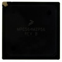
MPC564MZP56 Freescale Semiconductor, MPC564MZP56 Datasheet - Page 947

MPC564MZP56
Manufacturer Part Number
MPC564MZP56
Description
IC MCU 512K FLASH 56MHZ 388-BGA
Manufacturer
Freescale Semiconductor
Series
MPC5xxr
Specifications of MPC564MZP56
Core Processor
PowerPC
Core Size
32-Bit
Speed
56MHz
Connectivity
CAN, EBI/EMI, SCI, SPI, UART/USART
Peripherals
POR, PWM, WDT
Number Of I /o
56
Program Memory Size
512KB (512K x 8)
Program Memory Type
FLASH
Ram Size
32K x 8
Voltage - Supply (vcc/vdd)
2.5 V ~ 2.7 V
Data Converters
A/D 32x10b
Oscillator Type
External
Operating Temperature
-40°C ~ 125°C
Package / Case
388-BGA
Core
PowerPC
Processor Series
MPC5xx
Data Bus Width
32 bit
Maximum Clock Frequency
56 MHz
Data Ram Size
32 KB
On-chip Adc
Yes
Number Of Programmable I/os
56
Number Of Timers
2
Operating Supply Voltage
0 V to 5 V
Mounting Style
SMD/SMT
A/d Bit Size
10 bit
A/d Channels Available
32
Height
1.95 mm
Interface Type
CAN, JTAG, QSPI, SCI, SPI, UART
Length
27 mm
Maximum Operating Temperature
+ 125 C
Minimum Operating Temperature
- 40 C
Supply Voltage (max)
2.7 V, 5.25 V
Supply Voltage (min)
2.5 V, 4.75 V
Width
27 mm
For Use With
MPC564EVB - KIT EVAL FOR MPC561/562/563/564
Lead Free Status / RoHS Status
Contains lead / RoHS non-compliant
Eeprom Size
-
Lead Free Status / Rohs Status
No RoHS Version Available
Available stocks
Company
Part Number
Manufacturer
Quantity
Price
Company:
Part Number:
MPC564MZP56
Manufacturer:
FREESCAL
Quantity:
364
Company:
Part Number:
MPC564MZP56
Manufacturer:
Freescale Semiconductor
Quantity:
10 000
Part Number:
MPC564MZP56
Manufacturer:
FREESCALE
Quantity:
20 000
Company:
Part Number:
MPC564MZP56R2
Manufacturer:
Freescale Semiconductor
Quantity:
10 000
- Current page: 947 of 1420
- Download datasheet (11Mb)
23.4.6.5
When not in debug mode the development port starts communications by setting DSDO (the MSB of the
35-bit development port shift register) low to indicate that all activity related to the previous transmission
are complete and that a new transmission may begin. The start of a serial transmission from an external
development tool to the development port is signaled by a start bit. A mode bit in the transmission defines
the transmission as either a trap enable mode transmission or a debug mode transmission. If the mode bit
is set the transmission will only be 10 bits long and only seven data bits will be shifted into the shift
register. These seven bits will be latched into the TECR. A control bit determines whether the data is
latched into the trap enable and VSYNC bits of the TECR or into the breakpoints bits of the TECR.
23.4.6.6
The development port shift register is 35 bits wide but trap enable mode transmissions only use the
start/ready bit, a mode/status bit, a control/status bit, and the seven least significant data bits. The encoding
of data shifted into the development port shift register (through the DSDI pin) is shown in
Table 23-11
Freescale Semiconductor
CLKOUT
SRESET
First Start bit detected after DSDI negation (self clocked mode)
CLKEN
Internal clock enable signal asserts 8 clocks after SRESET
DSDI
negation if DSDI is negated. This enables clocked mode.
below:
Development Port Serial Communications — Trap Enable Mode
Serial Data into Development Port — Trap Enable Mode
DSDI negates following SRESET negation
to enable clocked mode.
0
1
Figure 23-11. Enabling Clock Mode Following Reset
2
MPC561/MPC563 Reference Manual, Rev. 1.2
3
4
5
6
7
8
9
10
11
12
13 14
15
Development Support
Table 23-10
23-33
and
Related parts for MPC564MZP56
Image
Part Number
Description
Manufacturer
Datasheet
Request
R

Part Number:
Description:
MPC5 1K0 5%
Manufacturer:
TE Connectivity
Datasheet:

Part Number:
Description:
MPC5 500R 5%
Manufacturer:
TE Connectivity
Datasheet:

Part Number:
Description:
MPC5 5K0 5%
Manufacturer:
Tyco Electronics
Datasheet:

Part Number:
Description:
MPC5 5R0 5%
Manufacturer:
Tyco Electronics
Datasheet:

Part Number:
Description:
MPC5 50K 5%
Manufacturer:
Tyco Electronics
Datasheet:

Part Number:
Description:
MPC5 1R0 5%
Manufacturer:
Tyco Electronics
Datasheet:
Part Number:
Description:
Manufacturer:
Freescale Semiconductor, Inc
Datasheet:
Part Number:
Description:
Manufacturer:
Freescale Semiconductor, Inc
Datasheet:
Part Number:
Description:
Manufacturer:
Freescale Semiconductor, Inc
Datasheet:
Part Number:
Description:
Manufacturer:
Freescale Semiconductor, Inc
Datasheet:
Part Number:
Description:
Manufacturer:
Freescale Semiconductor, Inc
Datasheet:


