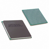
EP1SGX10DF672C5N Altera, EP1SGX10DF672C5N Datasheet - Page 156

EP1SGX10DF672C5N
Manufacturer Part Number
EP1SGX10DF672C5N
Description
IC STRATIX GX FPGA 10KLE 672FBGA
Manufacturer
Altera
Series
Stratix® GXr
Datasheet
1.EP1SGX10CF672C7N.pdf
(272 pages)
Specifications of EP1SGX10DF672C5N
Number Of Logic Elements/cells
10570
Number Of Labs/clbs
1057
Total Ram Bits
920448
Number Of I /o
362
Voltage - Supply
1.425 V ~ 1.575 V
Mounting Type
Surface Mount
Operating Temperature
0°C ~ 85°C
Package / Case
672-FBGA
Lead Free Status / RoHS Status
Lead free / RoHS Compliant
Number Of Gates
-
Available stocks
Company
Part Number
Manufacturer
Quantity
Price
- Current page: 156 of 272
- Download datasheet (3Mb)
PLLs & Clock Networks
4–90
Stratix GX Device Handbook, Volume 1
■
■
Phase & Delay Shifting
Stratix GX device enhanced PLLs provide advanced programmable
phase and clock delay shifting. For phase shifting, you can specify a
phase shift (in degrees or time units) for each PLL clock output port or for
all outputs together in one shift. Phase-shifting values in time units are
allowed with a resolution range of 160 to 420 ps. This resolution is a
function of frequency input and the multiplication and division factors.
In other words, it is a function of the VCO period equal to one-eighth of
the VCO period. Each clock output counter can choose a different phase
of the VCO period from up to eight taps. You can use this clock output
counter along with an initial setting on the post-scale counter to achieve
a phase-shift range for the entire period of the output clock. The phase tap
feedback to the m counter can shift all outputs to a single phase or delay.
The Quartus II software automatically sets the phase taps and counter
settings according to the phase shift entered.
In addition to the phase-shift feature, the fine tune clock delay shift
feature provides advanced time delay shift control on each of the four
PLL outputs. Each PLL output shifts in 250-ps increments for a range of
–3.0 ns to +3.0 ns between any two outputs using discrete delay elements.
Total delay shift between any two PLL outputs must be less than 3 ns. For
example, shifts on outputs of –1 and +2 ns is allowed, but not –1 and
+2.5 ns. There is some delay variation due to process, voltage, and
temperature. Only the clock delay shift blocks can be controlled during
system operation for dynamic clock delay control.
Spread-Spectrum Clocking
The Stratix GX device’s enhanced PLLs use spread-spectrum technology
to reduce electromagnetic interference generation from a system by
distributing the energy over a broader frequency range. The enhanced
feedback for one of the dedicated external outputs, either one
single-ended or one differential pair. In this mode, one e counter
feeds back to the PLL FBIN input, becoming part of the feedback
loop.
Normal mode: If an internal clock is used in this mode, it is
phase-aligned to the input clock pin. The external clock output pin
has a phase delay relative to the clock input pin if connected in this
mode. You define which internal clock output from the PLL should
be phase-aligned to the internal clock pin.
No compensation: In this mode, the PLL does not compensate for
any clock networks or external clock outputs.
Altera Corporation
February 2005
Related parts for EP1SGX10DF672C5N
Image
Part Number
Description
Manufacturer
Datasheet
Request
R

Part Number:
Description:
CYCLONE II STARTER KIT EP2C20N
Manufacturer:
Altera
Datasheet:

Part Number:
Description:
CPLD, EP610 Family, ECMOS Process, 300 Gates, 16 Macro Cells, 16 Reg., 16 User I/Os, 5V Supply, 35 Speed Grade, 24DIP
Manufacturer:
Altera Corporation
Datasheet:

Part Number:
Description:
CPLD, EP610 Family, ECMOS Process, 300 Gates, 16 Macro Cells, 16 Reg., 16 User I/Os, 5V Supply, 15 Speed Grade, 24DIP
Manufacturer:
Altera Corporation
Datasheet:

Part Number:
Description:
Manufacturer:
Altera Corporation
Datasheet:

Part Number:
Description:
CPLD, EP610 Family, ECMOS Process, 300 Gates, 16 Macro Cells, 16 Reg., 16 User I/Os, 5V Supply, 30 Speed Grade, 24DIP
Manufacturer:
Altera Corporation
Datasheet:

Part Number:
Description:
High-performance, low-power erasable programmable logic devices with 8 macrocells, 10ns
Manufacturer:
Altera Corporation
Datasheet:

Part Number:
Description:
High-performance, low-power erasable programmable logic devices with 8 macrocells, 7ns
Manufacturer:
Altera Corporation
Datasheet:

Part Number:
Description:
Classic EPLD
Manufacturer:
Altera Corporation
Datasheet:

Part Number:
Description:
High-performance, low-power erasable programmable logic devices with 8 macrocells, 10ns
Manufacturer:
Altera Corporation
Datasheet:

Part Number:
Description:
Manufacturer:
Altera Corporation
Datasheet:

Part Number:
Description:
Manufacturer:
Altera Corporation
Datasheet:

Part Number:
Description:
Manufacturer:
Altera Corporation
Datasheet:

Part Number:
Description:
CPLD, EP610 Family, ECMOS Process, 300 Gates, 16 Macro Cells, 16 Reg., 16 User I/Os, 5V Supply, 25 Speed Grade, 24DIP
Manufacturer:
Altera Corporation
Datasheet:


