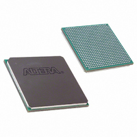
EP1SGX10DF672C5N Altera, EP1SGX10DF672C5N Datasheet - Page 64

EP1SGX10DF672C5N
Manufacturer Part Number
EP1SGX10DF672C5N
Description
IC STRATIX GX FPGA 10KLE 672FBGA
Manufacturer
Altera
Series
Stratix® GXr
Datasheet
1.EP1SGX10CF672C7N.pdf
(272 pages)
Specifications of EP1SGX10DF672C5N
Number Of Logic Elements/cells
10570
Number Of Labs/clbs
1057
Total Ram Bits
920448
Number Of I /o
362
Voltage - Supply
1.425 V ~ 1.575 V
Mounting Type
Surface Mount
Operating Temperature
0°C ~ 85°C
Package / Case
672-FBGA
Lead Free Status / RoHS Status
Lead free / RoHS Compliant
Number Of Gates
-
Available stocks
Company
Part Number
Manufacturer
Quantity
Price
- Current page: 64 of 272
- Download datasheet (3Mb)
Introduction
Figure 3–11. DPA Data Realigner
3–14
Stratix GX Device Handbook, Volume 1
Register 2
D10 is the upcoming
Bit Slip
Zero bits slipped.
D19
D18
D17
D16
D15
D14
D13
D12
D11
D10
bit to be slipped.
Counter = 0
Register 3
Bit Slip
D9
D8
D7
D6
D5
D4
D3
D2
D1
D0
One bit
slipped
Register 2
D21 is the upcoming
Bit Slip
D29
D28
D27
D26
D25
D24
D23
D22
D21
D20
bit to be slipped.
One bit slipped.
Counter = 1
The DPA data-realignment circuitry allows further realignment beyond
what the J multiplication factor allows. You can set the J multiplication
factor to be 8 or 10. However, because data must be continuously clocked
in on each low-speed clock cycle, the upcoming bit to be realigned and
previous n − 1 bits of data are selected each time the data realignment
logic’s counter passes n − 1. At this point the data is selected entirely from
bit-slip register 3 (see
array receives a new valid byte of data on the next divided low speed
clock cycle.
selection from data in the data realignment register 2 and data
realignment register 3 based on its current counter value upon
continuous request of data slipping from the logic array.
Use the rx_channel_data_align signal within the device to activate
the data realigner. You can use internal logic or an external pin to control
the rx_channel_data_align signal. To ensure the rising edge of the
rx_channel_data_align signal is latched into the control logic, the
rx_channel_data_align signal should stay high for at least two low-
frequency clock cycles.
Register 3
Bit Slip
D19
D18
D17
D16
D15
D14
D13
D12
D11
D10
Seven more
bits slipped
Figure 3–11
Register 2
D98 is the upcoming
Bit Slip
Eight bits slipped.
bit to be slipped.
D99
D98
D97
D96
D95
D94
D93
D92
D91
D90
Counter = 8
Figure
Register 3
shows the data realignment logic output
Bit Slip
D89
D18
D87
D86
D85
D84
D83
D82
D81
D80
3–11) as the counter is reset to 0. The logic
One more
bit slipped
Register 2
D119 is the upcoming
Bit Slip
D119
D118
D117
D116
D115
D114
D113
D112
D111
D110
Nine bits slipped.
bit to be slipped.
Counter = 9
Register 3
Bit Slip
D99
D98
D97
D96
D95
D94
D93
D92
D91
D90
One more
bit slipped
Altera Corporation
Register 2
Real data will resume
Bit Slip
D119
D118
D117
D116
D115
D114
D113
D112
D111
D110
on the next byte.
August 2005
10 bits slipped.
Counter = 0
Register 3
Bit Slip
D109
D108
D107
D106
D125
D124
D123
D102
D101
D100
Related parts for EP1SGX10DF672C5N
Image
Part Number
Description
Manufacturer
Datasheet
Request
R

Part Number:
Description:
CYCLONE II STARTER KIT EP2C20N
Manufacturer:
Altera
Datasheet:

Part Number:
Description:
CPLD, EP610 Family, ECMOS Process, 300 Gates, 16 Macro Cells, 16 Reg., 16 User I/Os, 5V Supply, 35 Speed Grade, 24DIP
Manufacturer:
Altera Corporation
Datasheet:

Part Number:
Description:
CPLD, EP610 Family, ECMOS Process, 300 Gates, 16 Macro Cells, 16 Reg., 16 User I/Os, 5V Supply, 15 Speed Grade, 24DIP
Manufacturer:
Altera Corporation
Datasheet:

Part Number:
Description:
Manufacturer:
Altera Corporation
Datasheet:

Part Number:
Description:
CPLD, EP610 Family, ECMOS Process, 300 Gates, 16 Macro Cells, 16 Reg., 16 User I/Os, 5V Supply, 30 Speed Grade, 24DIP
Manufacturer:
Altera Corporation
Datasheet:

Part Number:
Description:
High-performance, low-power erasable programmable logic devices with 8 macrocells, 10ns
Manufacturer:
Altera Corporation
Datasheet:

Part Number:
Description:
High-performance, low-power erasable programmable logic devices with 8 macrocells, 7ns
Manufacturer:
Altera Corporation
Datasheet:

Part Number:
Description:
Classic EPLD
Manufacturer:
Altera Corporation
Datasheet:

Part Number:
Description:
High-performance, low-power erasable programmable logic devices with 8 macrocells, 10ns
Manufacturer:
Altera Corporation
Datasheet:

Part Number:
Description:
Manufacturer:
Altera Corporation
Datasheet:

Part Number:
Description:
Manufacturer:
Altera Corporation
Datasheet:

Part Number:
Description:
Manufacturer:
Altera Corporation
Datasheet:

Part Number:
Description:
CPLD, EP610 Family, ECMOS Process, 300 Gates, 16 Macro Cells, 16 Reg., 16 User I/Os, 5V Supply, 25 Speed Grade, 24DIP
Manufacturer:
Altera Corporation
Datasheet:


