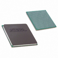
EP1SGX10DF672C5N Altera, EP1SGX10DF672C5N Datasheet - Page 266

EP1SGX10DF672C5N
Manufacturer Part Number
EP1SGX10DF672C5N
Description
IC STRATIX GX FPGA 10KLE 672FBGA
Manufacturer
Altera
Series
Stratix® GXr
Datasheet
1.EP1SGX10CF672C7N.pdf
(272 pages)
Specifications of EP1SGX10DF672C5N
Number Of Logic Elements/cells
10570
Number Of Labs/clbs
1057
Total Ram Bits
920448
Number Of I /o
362
Voltage - Supply
1.425 V ~ 1.575 V
Mounting Type
Surface Mount
Operating Temperature
0°C ~ 85°C
Package / Case
672-FBGA
Lead Free Status / RoHS Status
Lead free / RoHS Compliant
Number Of Gates
-
Available stocks
Company
Part Number
Manufacturer
Quantity
Price
- Current page: 266 of 272
- Download datasheet (3Mb)
High-Speed I/O Specification
6–64
Stratix GX Device Handbook, Volume 1
f
f
t
t
t
t
t
t
t
f
t
t
f
% spread
t
f
f
f
t
t
OUT
OUT_EXT
OUTDUTY
JITTER
CONFIG5,6
CONFIG11,12
SCANCLK
DLOCK
LOCK
VCO
LSKEW
SKEW
SS
ARESET
IN
INDUTY
EINDUTY
INJITTER
EINJITTER
Table 6–89. Enhanced PLL Specifications for -6 Speed Grades
Table 6–90. Enhanced PLL Specifications for -7 Speed Grade (Part 1 of 3)
Symbol
Symbol
Output frequency for internal global or
regional clock
Output frequency for external clock
Duty cycle for external clock output
(when set to 50%)
Period jitter for external clock output
Time required to reconfigure the scan
chains for PLLs 5 and 6
Time required to reconfigure the scan
chains for PLLs 11 and 12
scanclk frequency
Time required to lock dynamically (after
switchover or reconfiguring any non-
post-scale counters/delays)
Time required to lock from end of
device configuration
PLL internal VCO operating range
Clock skew between two external clock
outputs driven by the same counter
Clock skew between two external clock
outputs driven by the different counters
with the same settings
Spread spectrum modulation frequency
Percentage spread for spread
spectrum frequency
Minimum pulse width on
signal
Input clock frequency
Input clock duty cycle
External feedback clock input duty
cycle
Input clock period jitter
External feedback clock period jitter
Parameter
Parameter
(9)
(4)
(10)
areset
(6) (10)
(2)
(5)
Min Typ
3
300
Min
0.3
0.3
0.4
(8)
45
10
30
10
40
40
(1)
±50
±75
0.5
Typ
(Part 2 of 2)
±20 mUI for <200 MHz outclk
±100 ps for >200 MHz outclk
289/f
193/f
±200
±200
800
Max
450
500
100
400
150
0.6
Max
55
22
565
SCANCLK
SCANCLK
60
60
(7)
(2)
(2)
Altera Corporation
June 2006
ps or
MHz
MHz
MHz
MHz
Unit
mUI
kHz
MHz
Unit
ps
ps
ns
μs
μs
%
%
ps
ps
%
%
Related parts for EP1SGX10DF672C5N
Image
Part Number
Description
Manufacturer
Datasheet
Request
R

Part Number:
Description:
CYCLONE II STARTER KIT EP2C20N
Manufacturer:
Altera
Datasheet:

Part Number:
Description:
CPLD, EP610 Family, ECMOS Process, 300 Gates, 16 Macro Cells, 16 Reg., 16 User I/Os, 5V Supply, 35 Speed Grade, 24DIP
Manufacturer:
Altera Corporation
Datasheet:

Part Number:
Description:
CPLD, EP610 Family, ECMOS Process, 300 Gates, 16 Macro Cells, 16 Reg., 16 User I/Os, 5V Supply, 15 Speed Grade, 24DIP
Manufacturer:
Altera Corporation
Datasheet:

Part Number:
Description:
Manufacturer:
Altera Corporation
Datasheet:

Part Number:
Description:
CPLD, EP610 Family, ECMOS Process, 300 Gates, 16 Macro Cells, 16 Reg., 16 User I/Os, 5V Supply, 30 Speed Grade, 24DIP
Manufacturer:
Altera Corporation
Datasheet:

Part Number:
Description:
High-performance, low-power erasable programmable logic devices with 8 macrocells, 10ns
Manufacturer:
Altera Corporation
Datasheet:

Part Number:
Description:
High-performance, low-power erasable programmable logic devices with 8 macrocells, 7ns
Manufacturer:
Altera Corporation
Datasheet:

Part Number:
Description:
Classic EPLD
Manufacturer:
Altera Corporation
Datasheet:

Part Number:
Description:
High-performance, low-power erasable programmable logic devices with 8 macrocells, 10ns
Manufacturer:
Altera Corporation
Datasheet:

Part Number:
Description:
Manufacturer:
Altera Corporation
Datasheet:

Part Number:
Description:
Manufacturer:
Altera Corporation
Datasheet:

Part Number:
Description:
Manufacturer:
Altera Corporation
Datasheet:

Part Number:
Description:
CPLD, EP610 Family, ECMOS Process, 300 Gates, 16 Macro Cells, 16 Reg., 16 User I/Os, 5V Supply, 25 Speed Grade, 24DIP
Manufacturer:
Altera Corporation
Datasheet:


