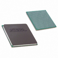
EP1SGX10DF672C5N Altera, EP1SGX10DF672C5N Datasheet - Page 188

EP1SGX10DF672C5N
Manufacturer Part Number
EP1SGX10DF672C5N
Description
IC STRATIX GX FPGA 10KLE 672FBGA
Manufacturer
Altera
Series
Stratix® GXr
Datasheet
1.EP1SGX10CF672C7N.pdf
(272 pages)
Specifications of EP1SGX10DF672C5N
Number Of Logic Elements/cells
10570
Number Of Labs/clbs
1057
Total Ram Bits
920448
Number Of I /o
362
Voltage - Supply
1.425 V ~ 1.575 V
Mounting Type
Surface Mount
Operating Temperature
0°C ~ 85°C
Package / Case
672-FBGA
Lead Free Status / RoHS Status
Lead free / RoHS Compliant
Number Of Gates
-
Available stocks
Company
Part Number
Manufacturer
Quantity
Price
- Current page: 188 of 272
- Download datasheet (3Mb)
IEEE Std. 1149.1 (JTAG) Boundary-Scan Support
IEEE Std. 1149.1
(JTAG)
Boundary-Scan
Support
4–122
Stratix GX Device Handbook, Volume 1
SAMPLE/PRELOAD
EXTEST
BYPASS
USERCODE
IDCODE
HIGHZ
Table 4–33. Stratix GX JTAG Instructions (Part 1 of 2)
JTAG Instruction
(1)
(1)
Allows a snapshot of signals at the device pins to be captured and examined during
normal device operation, and permits an initial data pattern to be output at the device pins.
Also used by the SignalTap
Allows the external circuitry and board-level interconnects to be tested by forcing a test
pattern at the output pins and capturing test results at the input pins.
Places the 1-bit bypass register between the TDI and TDO pins, which allows the BST data
to pass synchronously through selected devices to adjacent devices during normal device
operation.
Selects the 32-bit
allowing the
Selects the IDCODE register and places it between TDI and TDO, allowing the IDCODE
to be serially shifted out of TDO.
Places the 1-bit bypass register between the TDI and TDO pins, which allows the BST data
to pass synchronously through selected devices to adjacent devices during normal device
operation, while tri-stating all of the I/O pins.
All Stratix GX devices provide JTAG BST circuitry that complies with the
IEEE Std. 1149.1a-1990 specification. JTAG boundary-scan testing can be
performed either before or after, but not during configuration. Stratix GX
devices can also use the JTAG port for configuration together with either
the Quartus II software or hardware using either Jam Files (.jam) or Jam
Byte-Code Files (.jbc).
Stratix GX devices support IOE I/O standard setting reconfiguration
through the JTAG BST chain. The JTAG chain can update the I/O
standard for all input and output pins any time before or during user
mode. You can use this ability for JTAG testing before configuration when
some of the Stratix GX pins drive or receive from other devices on the
board using voltage-referenced standards. Because the Stratix GX device
may not be configured before JTAG testing, the I/O pins may not be
configured for appropriate electrical standards for chip-to-chip
communication. Programming those I/O standards via JTAG allows you
to fully test I/O connection to other devices.
The enhanced PLL reconfiguration bits are part of the JTAG chain before
configuration and after power-up. After device configuration, the PLL
reconfiguration bits are not part of the JTAG chain.
Stratix GX devices also use the JTAG port to monitor the logic operation
of the device with the SignalTap
devices support the JTAG instructions shown in
USERCODE
USERCODE
to be serially shifted out of TDO.
®
embedded logic analyzer.
register and places it between the TDI and TDO pins,
Description
®
embedded logic analyzer. Stratix GX
Table
4–33.
Altera Corporation
February 2005
Related parts for EP1SGX10DF672C5N
Image
Part Number
Description
Manufacturer
Datasheet
Request
R

Part Number:
Description:
CYCLONE II STARTER KIT EP2C20N
Manufacturer:
Altera
Datasheet:

Part Number:
Description:
CPLD, EP610 Family, ECMOS Process, 300 Gates, 16 Macro Cells, 16 Reg., 16 User I/Os, 5V Supply, 35 Speed Grade, 24DIP
Manufacturer:
Altera Corporation
Datasheet:

Part Number:
Description:
CPLD, EP610 Family, ECMOS Process, 300 Gates, 16 Macro Cells, 16 Reg., 16 User I/Os, 5V Supply, 15 Speed Grade, 24DIP
Manufacturer:
Altera Corporation
Datasheet:

Part Number:
Description:
Manufacturer:
Altera Corporation
Datasheet:

Part Number:
Description:
CPLD, EP610 Family, ECMOS Process, 300 Gates, 16 Macro Cells, 16 Reg., 16 User I/Os, 5V Supply, 30 Speed Grade, 24DIP
Manufacturer:
Altera Corporation
Datasheet:

Part Number:
Description:
High-performance, low-power erasable programmable logic devices with 8 macrocells, 10ns
Manufacturer:
Altera Corporation
Datasheet:

Part Number:
Description:
High-performance, low-power erasable programmable logic devices with 8 macrocells, 7ns
Manufacturer:
Altera Corporation
Datasheet:

Part Number:
Description:
Classic EPLD
Manufacturer:
Altera Corporation
Datasheet:

Part Number:
Description:
High-performance, low-power erasable programmable logic devices with 8 macrocells, 10ns
Manufacturer:
Altera Corporation
Datasheet:

Part Number:
Description:
Manufacturer:
Altera Corporation
Datasheet:

Part Number:
Description:
Manufacturer:
Altera Corporation
Datasheet:

Part Number:
Description:
Manufacturer:
Altera Corporation
Datasheet:

Part Number:
Description:
CPLD, EP610 Family, ECMOS Process, 300 Gates, 16 Macro Cells, 16 Reg., 16 User I/Os, 5V Supply, 25 Speed Grade, 24DIP
Manufacturer:
Altera Corporation
Datasheet:


