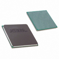
EP1SGX10DF672C5N Altera, EP1SGX10DF672C5N Datasheet - Page 51

EP1SGX10DF672C5N
Manufacturer Part Number
EP1SGX10DF672C5N
Description
IC STRATIX GX FPGA 10KLE 672FBGA
Manufacturer
Altera
Series
Stratix® GXr
Datasheet
1.EP1SGX10CF672C7N.pdf
(272 pages)
Specifications of EP1SGX10DF672C5N
Number Of Logic Elements/cells
10570
Number Of Labs/clbs
1057
Total Ram Bits
920448
Number Of I /o
362
Voltage - Supply
1.425 V ~ 1.575 V
Mounting Type
Surface Mount
Operating Temperature
0°C ~ 85°C
Package / Case
672-FBGA
Lead Free Status / RoHS Status
Lead free / RoHS Compliant
Number Of Gates
-
Available stocks
Company
Part Number
Manufacturer
Quantity
Price
- Current page: 51 of 272
- Download datasheet (3Mb)
Introduction
Altera Corporation
August 2005
SGX51003-1.1
Expansion in the telecommunications market and growth in Internet use
requires systems to move more data faster than ever. To meet this
demand, rely on solutions such as differential signaling and emerging
high-speed interface standards including RapidIO, POS-PHY 4, SFI-4, or
XSBI.
These new protocols support differential data rates up to 1 Gbps and
higher. At these high data rates, it becomes more challenging to manage
the skew between the clock and data signals. One solution to this
challenge is to use CDR to eliminate skew between data channels and
clock signals. Another potential solution, DPA, is beginning to be
incorporated into some of these protocols.
The source-synchronous high-speed interface in Stratix GX devices is a
dedicated circuit embedded into the PLD allowing for high-speed
communications. The High-Speed Source-Synchronous Differential I/O
Interfaces in Stratix GX Devices chapter of the Stratix GX Device Handbook,
Volume 2 provides information on the high-speed I/O standard features
and functions of the Stratix GX device.
Stratix GX I/O Banks
Stratix GX devices contain 17 I/O banks. I/O banks one and two support
high-speed LVDS, LVPECL, and 3.3-V PCML inputs and outputs. These
two banks also incorporate an embedded dynamic phase aligner within
the source-synchronous interface (see
dynamic phase aligner corrects for the phase difference between the clock
and data lines caused by skew. The dynamic phase aligner operates
automatically and continuously without requiring a fixed training
pattern, and allows the source-synchronous circuitry to capture data
correctly regardless of the channel-to-clock skew.
Principles of SERDES Operation
Stratix GX devices support source-synchronous differential signaling up
to 1 Gbps in DPA mode, and up to 840 Mbps in non-DPA mode. Serial
data is transmitted and received along with a low-frequency clock. The
PLL can multiply the incoming low-frequency clock by a factor of 1 to 10.
The SERDES factor J can be 8 or 10 for the DPA mode, or 4, 7, 8, or 10 for
all other modes. The SERDES factor does not have to equal the clock
3. Source-Synchronous
Signaling With DPA
Figure 3–8 on page
3–10). The
3–1
Related parts for EP1SGX10DF672C5N
Image
Part Number
Description
Manufacturer
Datasheet
Request
R

Part Number:
Description:
CYCLONE II STARTER KIT EP2C20N
Manufacturer:
Altera
Datasheet:

Part Number:
Description:
CPLD, EP610 Family, ECMOS Process, 300 Gates, 16 Macro Cells, 16 Reg., 16 User I/Os, 5V Supply, 35 Speed Grade, 24DIP
Manufacturer:
Altera Corporation
Datasheet:

Part Number:
Description:
CPLD, EP610 Family, ECMOS Process, 300 Gates, 16 Macro Cells, 16 Reg., 16 User I/Os, 5V Supply, 15 Speed Grade, 24DIP
Manufacturer:
Altera Corporation
Datasheet:

Part Number:
Description:
Manufacturer:
Altera Corporation
Datasheet:

Part Number:
Description:
CPLD, EP610 Family, ECMOS Process, 300 Gates, 16 Macro Cells, 16 Reg., 16 User I/Os, 5V Supply, 30 Speed Grade, 24DIP
Manufacturer:
Altera Corporation
Datasheet:

Part Number:
Description:
High-performance, low-power erasable programmable logic devices with 8 macrocells, 10ns
Manufacturer:
Altera Corporation
Datasheet:

Part Number:
Description:
High-performance, low-power erasable programmable logic devices with 8 macrocells, 7ns
Manufacturer:
Altera Corporation
Datasheet:

Part Number:
Description:
Classic EPLD
Manufacturer:
Altera Corporation
Datasheet:

Part Number:
Description:
High-performance, low-power erasable programmable logic devices with 8 macrocells, 10ns
Manufacturer:
Altera Corporation
Datasheet:

Part Number:
Description:
Manufacturer:
Altera Corporation
Datasheet:

Part Number:
Description:
Manufacturer:
Altera Corporation
Datasheet:

Part Number:
Description:
Manufacturer:
Altera Corporation
Datasheet:

Part Number:
Description:
CPLD, EP610 Family, ECMOS Process, 300 Gates, 16 Macro Cells, 16 Reg., 16 User I/Os, 5V Supply, 25 Speed Grade, 24DIP
Manufacturer:
Altera Corporation
Datasheet:


