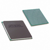
EP1SGX10DF672C5N Altera, EP1SGX10DF672C5N Datasheet - Page 170

EP1SGX10DF672C5N
Manufacturer Part Number
EP1SGX10DF672C5N
Description
IC STRATIX GX FPGA 10KLE 672FBGA
Manufacturer
Altera
Series
Stratix® GXr
Datasheet
1.EP1SGX10CF672C7N.pdf
(272 pages)
Specifications of EP1SGX10DF672C5N
Number Of Logic Elements/cells
10570
Number Of Labs/clbs
1057
Total Ram Bits
920448
Number Of I /o
362
Voltage - Supply
1.425 V ~ 1.575 V
Mounting Type
Surface Mount
Operating Temperature
0°C ~ 85°C
Package / Case
672-FBGA
Lead Free Status / RoHS Status
Lead free / RoHS Compliant
Number Of Gates
-
Available stocks
Company
Part Number
Manufacturer
Quantity
Price
- Current page: 170 of 272
- Download datasheet (3Mb)
I/O Structure
Figure 4–64. Stratix GX IOE in DDR Input I/O Configuration
Notes to
(1)
(2)
(3)
4–104
Stratix GX Device Handbook, Volume 1
Column or Row
Interconnect
All input signals to the IOE can be inverted at the IOE.
This signal connection is only allowed on dedicated DQ function pins.
This signal is for dedicated DQS function pins only.
I/O Interconnect
Figure
[15..0]
4–64:
ioe_clk[7..0]
(1)
DQS Local
Bus (1), (2)
(1)
When using the IOE for DDR inputs, the two input registers clock double
rate input data on alternating edges. An input latch is also used within the
IOE for DDR input acquisition. The latch holds the data that is present
during the clock high times. This allows both bits of data to be
synchronous with the same clock edge (either rising or falling).
Figure 4–64
the DDR input timing diagram.
sclr
clkin
aclr/prn
Chip-Wide Reset
Enable Delay
Output Clock
shows an IOE configured for DDR input.
Input Register
Input Register
CLRN/PRN
D
ENA
CLRN/PRN
D
ENA
Input Register Delay
Input Pin to
Q
Q
Note (1)
D
ENA
CLRN/PRN
To DQS Local
Latch
Bus (3)
Q
VCCIO
Figure 4–65
Altera Corporation
VCCIO
Optional
PCI Clamp
February 2005
Bus-Hold
Circuit
Programmable
Pull-Up
Resistor
shows
Related parts for EP1SGX10DF672C5N
Image
Part Number
Description
Manufacturer
Datasheet
Request
R

Part Number:
Description:
CYCLONE II STARTER KIT EP2C20N
Manufacturer:
Altera
Datasheet:

Part Number:
Description:
CPLD, EP610 Family, ECMOS Process, 300 Gates, 16 Macro Cells, 16 Reg., 16 User I/Os, 5V Supply, 35 Speed Grade, 24DIP
Manufacturer:
Altera Corporation
Datasheet:

Part Number:
Description:
CPLD, EP610 Family, ECMOS Process, 300 Gates, 16 Macro Cells, 16 Reg., 16 User I/Os, 5V Supply, 15 Speed Grade, 24DIP
Manufacturer:
Altera Corporation
Datasheet:

Part Number:
Description:
Manufacturer:
Altera Corporation
Datasheet:

Part Number:
Description:
CPLD, EP610 Family, ECMOS Process, 300 Gates, 16 Macro Cells, 16 Reg., 16 User I/Os, 5V Supply, 30 Speed Grade, 24DIP
Manufacturer:
Altera Corporation
Datasheet:

Part Number:
Description:
High-performance, low-power erasable programmable logic devices with 8 macrocells, 10ns
Manufacturer:
Altera Corporation
Datasheet:

Part Number:
Description:
High-performance, low-power erasable programmable logic devices with 8 macrocells, 7ns
Manufacturer:
Altera Corporation
Datasheet:

Part Number:
Description:
Classic EPLD
Manufacturer:
Altera Corporation
Datasheet:

Part Number:
Description:
High-performance, low-power erasable programmable logic devices with 8 macrocells, 10ns
Manufacturer:
Altera Corporation
Datasheet:

Part Number:
Description:
Manufacturer:
Altera Corporation
Datasheet:

Part Number:
Description:
Manufacturer:
Altera Corporation
Datasheet:

Part Number:
Description:
Manufacturer:
Altera Corporation
Datasheet:

Part Number:
Description:
CPLD, EP610 Family, ECMOS Process, 300 Gates, 16 Macro Cells, 16 Reg., 16 User I/Os, 5V Supply, 25 Speed Grade, 24DIP
Manufacturer:
Altera Corporation
Datasheet:


