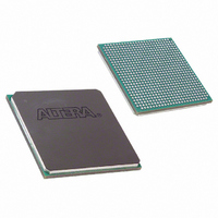
EP1SGX10DF672C5N Altera, EP1SGX10DF672C5N Datasheet - Page 97

EP1SGX10DF672C5N
Manufacturer Part Number
EP1SGX10DF672C5N
Description
IC STRATIX GX FPGA 10KLE 672FBGA
Manufacturer
Altera
Series
Stratix® GXr
Datasheet
1.EP1SGX10CF672C7N.pdf
(272 pages)
Specifications of EP1SGX10DF672C5N
Number Of Logic Elements/cells
10570
Number Of Labs/clbs
1057
Total Ram Bits
920448
Number Of I /o
362
Voltage - Supply
1.425 V ~ 1.575 V
Mounting Type
Surface Mount
Operating Temperature
0°C ~ 85°C
Package / Case
672-FBGA
Lead Free Status / RoHS Status
Lead free / RoHS Compliant
Number Of Gates
-
Available stocks
Company
Part Number
Manufacturer
Quantity
Price
- Current page: 97 of 272
- Download datasheet (3Mb)
Altera Corporation
February 2005
The read and write operation of the memory is controlled by the WREN
signal, which sets the ports into either read or write modes. There is no
separate read enable (RE) signal.
Writing into RAM is controlled by both the WREN and byte enable
(byteena) signals for each port. The default value for the byteena
signal is high, in which case writing is controlled only by the WREN signal.
The byte enables are available for the ×18, ×36, and ×72 modes. In the
×144 simple dual-port mode, the two sets of byteena signals
(byteena_a and byteena_b) are combined to form the necessary
16 byte enables.
64K
32K
16K
8K
Table 4–8. M-RAM Block Configurations (True Dual-Port)
Table 4–9. Byte Enable for M-RAM Blocks
byteena[3..0]
×
×
×
×
72
[0] = 1
[1] = 1
[2] = 1
[3] = 1
[4] = 1
[5] = 1
[6] = 1
[7] = 1
9
18
36
Port A
Tables 4–9
datain ×18
[17..9]
64K × 9
[8..0]
–
–
–
–
–
–
v
v
v
v
and
4–10
Stratix GX Device Handbook, Volume 1
summarize the byte selection.
32K × 18
v
v
v
v
Notes
datain ×36
[26..18]
[35..27]
[17..9]
[8..0]
Port B
–
–
–
–
(1),
16K × 36
(2)
Stratix GX Architecture
v
v
v
v
datain ×72
[26..18]
[35..27]
[44..36]
[53..45]
[62..54]
[71..63]
[17..9]
[8..0]
8K × 72
v
v
v
v
4–31
Related parts for EP1SGX10DF672C5N
Image
Part Number
Description
Manufacturer
Datasheet
Request
R

Part Number:
Description:
CYCLONE II STARTER KIT EP2C20N
Manufacturer:
Altera
Datasheet:

Part Number:
Description:
CPLD, EP610 Family, ECMOS Process, 300 Gates, 16 Macro Cells, 16 Reg., 16 User I/Os, 5V Supply, 35 Speed Grade, 24DIP
Manufacturer:
Altera Corporation
Datasheet:

Part Number:
Description:
CPLD, EP610 Family, ECMOS Process, 300 Gates, 16 Macro Cells, 16 Reg., 16 User I/Os, 5V Supply, 15 Speed Grade, 24DIP
Manufacturer:
Altera Corporation
Datasheet:

Part Number:
Description:
Manufacturer:
Altera Corporation
Datasheet:

Part Number:
Description:
CPLD, EP610 Family, ECMOS Process, 300 Gates, 16 Macro Cells, 16 Reg., 16 User I/Os, 5V Supply, 30 Speed Grade, 24DIP
Manufacturer:
Altera Corporation
Datasheet:

Part Number:
Description:
High-performance, low-power erasable programmable logic devices with 8 macrocells, 10ns
Manufacturer:
Altera Corporation
Datasheet:

Part Number:
Description:
High-performance, low-power erasable programmable logic devices with 8 macrocells, 7ns
Manufacturer:
Altera Corporation
Datasheet:

Part Number:
Description:
Classic EPLD
Manufacturer:
Altera Corporation
Datasheet:

Part Number:
Description:
High-performance, low-power erasable programmable logic devices with 8 macrocells, 10ns
Manufacturer:
Altera Corporation
Datasheet:

Part Number:
Description:
Manufacturer:
Altera Corporation
Datasheet:

Part Number:
Description:
Manufacturer:
Altera Corporation
Datasheet:

Part Number:
Description:
Manufacturer:
Altera Corporation
Datasheet:

Part Number:
Description:
CPLD, EP610 Family, ECMOS Process, 300 Gates, 16 Macro Cells, 16 Reg., 16 User I/Os, 5V Supply, 25 Speed Grade, 24DIP
Manufacturer:
Altera Corporation
Datasheet:


