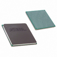
EP1SGX10DF672C5N Altera, EP1SGX10DF672C5N Datasheet - Page 174

EP1SGX10DF672C5N
Manufacturer Part Number
EP1SGX10DF672C5N
Description
IC STRATIX GX FPGA 10KLE 672FBGA
Manufacturer
Altera
Series
Stratix® GXr
Datasheet
1.EP1SGX10CF672C7N.pdf
(272 pages)
Specifications of EP1SGX10DF672C5N
Number Of Logic Elements/cells
10570
Number Of Labs/clbs
1057
Total Ram Bits
920448
Number Of I /o
362
Voltage - Supply
1.425 V ~ 1.575 V
Mounting Type
Surface Mount
Operating Temperature
0°C ~ 85°C
Package / Case
672-FBGA
Lead Free Status / RoHS Status
Lead free / RoHS Compliant
Number Of Gates
-
Available stocks
Company
Part Number
Manufacturer
Quantity
Price
- Current page: 174 of 272
- Download datasheet (3Mb)
I/O Structure
4–108
Stratix GX Device Handbook, Volume 1
Notes to
(1)
(2)
(3)
(4)
(5)
(6)
(7)
DDR SDRAM (1),
DDR SDRAM - side banks (2), (3),
(4)
RLDRAM II
QDR SRAM
QDRII SRAM
ZBT SRAM
Table 4–22. External RAM Support in EP1SGX10 Through EP1SGX40 Devices
These maximum clock rates apply if the Stratix GX device uses DQS phase-shift circuitry to interface with DDR
SDRAM. DQS phase-shift circuitry is only available in the top and bottom I/O banks (I/O banks 3, 4, 7, and 8).
For more information on DDR SDRAM, see AN 342: Interfacing DDR SDRAM with Stratix & Stratix GX Devices.
DDR SDRAM is supported on the Stratix GX device side I/O banks (I/O banks 1, 2, 5, and 6) without dedicated
DQS phase-shift circuitry. The read DQS signal is ignored in this mode.
These performance specifications are preliminary.
This device does not support RLDRAM II.
For more information on QDR or QDRII SRAM, see AN 349: QDR SRAM Controller Reference Design for Stratix &
Stratix GX Devices.
For more information on ZBT SRAM, see AN 329: ZBT SRAM Controller Reference Design for Stratix & Stratix GX
Devices.
DDR Memory Type
Table
(4)
(7)
(6)
(6)
4–22:
(2)
Table 4–22
RLDRAM II, QDR SRAM, QDRII SRAM, and ZBT SRAM interfaces in
EP1SGX10 through EP1SGX40 devices. The DDR SDRAM and QDR
SRAM numbers in
characterization with third-party DDR SDRAM and QDR SRAM devices
over temperature and voltage extremes.
In addition to six I/O registers and one input latch in the IOE for
interfacing to these high-speed memory interfaces, Stratix GX devices
also have dedicated circuitry for interfacing with DDR SDRAM. In every
Stratix GX device, the I/O banks at the top (I/O banks 3 and 4) and
bottom (I/O banks 7 and 8) of the device support DDR SDRAM up to 200
MHz. These pins support DQS signals with DQ bus modes of ×8, ×16, or
×32.
SSTL-2
SSTL-2
1.8-V HSTL
1.5-V HSTL
1.5-V HSTL
LVTTL
I/O Standard
shows the performance specification for DDR SDRAM,
Table 4–22
-5 Speed Grade -6 Speed Grade
have been verified with hardware
200
150
200
167
200
200
Maximum Clock Rate (MHz)
167
133
167
167
200
(5)
Altera Corporation
February 2005
-7 Speed
Grade
133
133
133
133
167
(5)
Related parts for EP1SGX10DF672C5N
Image
Part Number
Description
Manufacturer
Datasheet
Request
R

Part Number:
Description:
CYCLONE II STARTER KIT EP2C20N
Manufacturer:
Altera
Datasheet:

Part Number:
Description:
CPLD, EP610 Family, ECMOS Process, 300 Gates, 16 Macro Cells, 16 Reg., 16 User I/Os, 5V Supply, 35 Speed Grade, 24DIP
Manufacturer:
Altera Corporation
Datasheet:

Part Number:
Description:
CPLD, EP610 Family, ECMOS Process, 300 Gates, 16 Macro Cells, 16 Reg., 16 User I/Os, 5V Supply, 15 Speed Grade, 24DIP
Manufacturer:
Altera Corporation
Datasheet:

Part Number:
Description:
Manufacturer:
Altera Corporation
Datasheet:

Part Number:
Description:
CPLD, EP610 Family, ECMOS Process, 300 Gates, 16 Macro Cells, 16 Reg., 16 User I/Os, 5V Supply, 30 Speed Grade, 24DIP
Manufacturer:
Altera Corporation
Datasheet:

Part Number:
Description:
High-performance, low-power erasable programmable logic devices with 8 macrocells, 10ns
Manufacturer:
Altera Corporation
Datasheet:

Part Number:
Description:
High-performance, low-power erasable programmable logic devices with 8 macrocells, 7ns
Manufacturer:
Altera Corporation
Datasheet:

Part Number:
Description:
Classic EPLD
Manufacturer:
Altera Corporation
Datasheet:

Part Number:
Description:
High-performance, low-power erasable programmable logic devices with 8 macrocells, 10ns
Manufacturer:
Altera Corporation
Datasheet:

Part Number:
Description:
Manufacturer:
Altera Corporation
Datasheet:

Part Number:
Description:
Manufacturer:
Altera Corporation
Datasheet:

Part Number:
Description:
Manufacturer:
Altera Corporation
Datasheet:

Part Number:
Description:
CPLD, EP610 Family, ECMOS Process, 300 Gates, 16 Macro Cells, 16 Reg., 16 User I/Os, 5V Supply, 25 Speed Grade, 24DIP
Manufacturer:
Altera Corporation
Datasheet:


