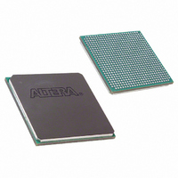
EP1SGX10DF672C5N Altera, EP1SGX10DF672C5N Datasheet - Page 206

EP1SGX10DF672C5N
Manufacturer Part Number
EP1SGX10DF672C5N
Description
IC STRATIX GX FPGA 10KLE 672FBGA
Manufacturer
Altera
Series
Stratix® GXr
Datasheet
1.EP1SGX10CF672C7N.pdf
(272 pages)
Specifications of EP1SGX10DF672C5N
Number Of Logic Elements/cells
10570
Number Of Labs/clbs
1057
Total Ram Bits
920448
Number Of I /o
362
Voltage - Supply
1.425 V ~ 1.575 V
Mounting Type
Surface Mount
Operating Temperature
0°C ~ 85°C
Package / Case
672-FBGA
Lead Free Status / RoHS Status
Lead free / RoHS Compliant
Number Of Gates
-
Available stocks
Company
Part Number
Manufacturer
Quantity
Price
- Current page: 206 of 272
- Download datasheet (3Mb)
Operating Conditions
6–4
Stratix GX Device Handbook, Volume 1
Notes to
(1)
(2)
(3)
(4)
(5)
(6)
(7)
(8)
(9)
(10) The device can tolerate prolonged operation at this absolute maximum, as long as the maximum specification is
(11) Each usable quad requires its own R
(12) The Stratix GX device’s recommended operating conditions do not include the transceiver. Refer to
(13) Minimum DC input to the transceiver pins is –0.5 V. During transitions, the transceiver pins may undershoot to
Refclkb
Power per
quadrant
(PCS +
PMA)
Symbol
Description
Table 6–6. Stratix GX Transceiver Block On-Chip Termination (Part 2 of 2)
Table 6–7. Stratix GX Transceiver Block AC Specification (Part 1 of 7)
Symbol /
See the
Conditions beyond those listed in
operation at the absolute maximum ratings for extended periods of time may have adverse affects on the device.
Minimum DC input is –0.5 V. During transitions, the inputs may undershoot to –2.0 V or overshoot to 4.6 V for
input currents less than 100 mA and periods shorter than 20 ns. (The information in this note does not include the
transceiver pins. See note
Maximum V
V
All pins, including dedicated inputs, clock, I/O, and JTAG pins, may be driven before V
powered.
Typical values are for T
This value is specified for normal device operation. The value may vary during power-up. This applies for all V
settings (3.3, 2.5, 1.8, and 1.5 V).
Pin pull-up resistance values decrease if an external source drives the pin higher than V
not violated.
device code means it has two usable quad so two different R
ground. The DC signal on the R
6–7.
–0.5 V or overshoot to 3.5 V for input currents less than 100 mA and periods shorter than 20 ns.
CCIO
Tables 6–1
Dedicated transceiver
clock termination
maximum and minimum conditions for LVPECL, LVDS, and 3.3-V PCML are shown in parentheses.
Operating Requirements for Altera Devices Data
3.125 Gbps, 400-
mV V
0 pre-emphasis
CC
Parameter
Conditions
rise time is 100 ms, and V
through 6–6:
o d
A
= 25° C, V
13
for information about the transient voltage on the transceiver pins.)
REF
Min
Commercial and industrial, 100-Ω setting
Commercial and industrial, 120-Ω setting
Commercial and industrial, 150-Ω setting
Speed Grade
Table 6–1
-5 Commercial
pin must be as clean as possible. Ensure that no noise is coupled to this pin.
CCINT
REF
450
Typ
resistor path to ground. For example, the “D” in the EP1SGX25DC1020
CC
= 1.5 V, and V
must rise monotonically.
may cause permanent damage to a device. Additionally, device
Max
(1)
Conditions
Sheet.
CCIO
Min
-6 Commercial &
Industrial Speed
= 1.5 V, 1.8 V, 2.5 V, and 3.3 V.
REF
pins must be connected to a R
450
Typ
Grade
(1)
Max
Min
103
120
149
Min
-7 Commercial &
Industrial Speed
CCIO
CCINT
108
128
158
Typ
Grade
Typ
.
(1)
Altera Corporation
and V
REF
resistor each to
Max
Max
113
134
167
Tables 6–4
CCIO
June 2006
are
Units
Unit
mW
Ω
Ω
Ω
CCIO
to
Related parts for EP1SGX10DF672C5N
Image
Part Number
Description
Manufacturer
Datasheet
Request
R

Part Number:
Description:
CYCLONE II STARTER KIT EP2C20N
Manufacturer:
Altera
Datasheet:

Part Number:
Description:
CPLD, EP610 Family, ECMOS Process, 300 Gates, 16 Macro Cells, 16 Reg., 16 User I/Os, 5V Supply, 35 Speed Grade, 24DIP
Manufacturer:
Altera Corporation
Datasheet:

Part Number:
Description:
CPLD, EP610 Family, ECMOS Process, 300 Gates, 16 Macro Cells, 16 Reg., 16 User I/Os, 5V Supply, 15 Speed Grade, 24DIP
Manufacturer:
Altera Corporation
Datasheet:

Part Number:
Description:
Manufacturer:
Altera Corporation
Datasheet:

Part Number:
Description:
CPLD, EP610 Family, ECMOS Process, 300 Gates, 16 Macro Cells, 16 Reg., 16 User I/Os, 5V Supply, 30 Speed Grade, 24DIP
Manufacturer:
Altera Corporation
Datasheet:

Part Number:
Description:
High-performance, low-power erasable programmable logic devices with 8 macrocells, 10ns
Manufacturer:
Altera Corporation
Datasheet:

Part Number:
Description:
High-performance, low-power erasable programmable logic devices with 8 macrocells, 7ns
Manufacturer:
Altera Corporation
Datasheet:

Part Number:
Description:
Classic EPLD
Manufacturer:
Altera Corporation
Datasheet:

Part Number:
Description:
High-performance, low-power erasable programmable logic devices with 8 macrocells, 10ns
Manufacturer:
Altera Corporation
Datasheet:

Part Number:
Description:
Manufacturer:
Altera Corporation
Datasheet:

Part Number:
Description:
Manufacturer:
Altera Corporation
Datasheet:

Part Number:
Description:
Manufacturer:
Altera Corporation
Datasheet:

Part Number:
Description:
CPLD, EP610 Family, ECMOS Process, 300 Gates, 16 Macro Cells, 16 Reg., 16 User I/Os, 5V Supply, 25 Speed Grade, 24DIP
Manufacturer:
Altera Corporation
Datasheet:


