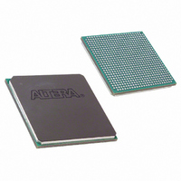
EP1SGX10DF672C5N Altera, EP1SGX10DF672C5N Datasheet - Page 169

EP1SGX10DF672C5N
Manufacturer Part Number
EP1SGX10DF672C5N
Description
IC STRATIX GX FPGA 10KLE 672FBGA
Manufacturer
Altera
Series
Stratix® GXr
Datasheet
1.EP1SGX10CF672C7N.pdf
(272 pages)
Specifications of EP1SGX10DF672C5N
Number Of Logic Elements/cells
10570
Number Of Labs/clbs
1057
Total Ram Bits
920448
Number Of I /o
362
Voltage - Supply
1.425 V ~ 1.575 V
Mounting Type
Surface Mount
Operating Temperature
0°C ~ 85°C
Package / Case
672-FBGA
Lead Free Status / RoHS Status
Lead free / RoHS Compliant
Number Of Gates
-
Available stocks
Company
Part Number
Manufacturer
Quantity
Price
- Current page: 169 of 272
- Download datasheet (3Mb)
Altera Corporation
February 2005
Programmable delays can increase the register-to-pin delays for output
and/or output enable registers. A programmable delay exists to increase
the t
Table 4–21
The IOE registers in Stratix GX devices share the same source for clear or
preset. You can program preset or clear for each individual IOE. You can
also program the registers to power up high or low after configuration is
complete. If programmed to power up low, an asynchronous clear can
control the registers. If programmed to power up high, an asynchronous
preset can control the registers. This feature prevents the inadvertent
activation of another device’s active-low input upon power-up. If one
register in an IOE uses a preset or clear signal then all registers in the IOE
must use that same signal if they require preset or clear. Additionally, a
synchronous reset signal is available for the IOE registers.
Double-Data Rate I/O Pins
Stratix GX devices have six registers in the IOE, which support DDR
interfacing by clocking data on both positive and negative clock edges.
The IOEs in Stratix GX devices support DDR inputs, DDR outputs, and
bidirectional DDR modes.
Input pin to logic array delay
Input pin to input register delay
Output pin delay
Output enable register t
Output t
Output clock enable delay
Input clock enable delay
Logic array to output register delay
Output enable clock enable delay
Table 4–21. Stratix GX Programmable Delay Chain
ZX
Programmable Delays
delay to the output pin, which is required for ZBT interfaces.
ZX
delay
shows the programmable delays for Stratix GX devices.
CO
delay
Decrease input delay to internal cells
Decrease input delay to input register
Increase delay to output pin
Increase delay to output enable pin
Increase t
Increase output clock enable delay
Increase input clock enable delay
Decrease input delay to output register
Increase output enable clock enable delay
Stratix GX Device Handbook, Volume 1
Quartus II Logic Option
ZX
delay to output pin
Stratix GX Architecture
4–103
Related parts for EP1SGX10DF672C5N
Image
Part Number
Description
Manufacturer
Datasheet
Request
R

Part Number:
Description:
CYCLONE II STARTER KIT EP2C20N
Manufacturer:
Altera
Datasheet:

Part Number:
Description:
CPLD, EP610 Family, ECMOS Process, 300 Gates, 16 Macro Cells, 16 Reg., 16 User I/Os, 5V Supply, 35 Speed Grade, 24DIP
Manufacturer:
Altera Corporation
Datasheet:

Part Number:
Description:
CPLD, EP610 Family, ECMOS Process, 300 Gates, 16 Macro Cells, 16 Reg., 16 User I/Os, 5V Supply, 15 Speed Grade, 24DIP
Manufacturer:
Altera Corporation
Datasheet:

Part Number:
Description:
Manufacturer:
Altera Corporation
Datasheet:

Part Number:
Description:
CPLD, EP610 Family, ECMOS Process, 300 Gates, 16 Macro Cells, 16 Reg., 16 User I/Os, 5V Supply, 30 Speed Grade, 24DIP
Manufacturer:
Altera Corporation
Datasheet:

Part Number:
Description:
High-performance, low-power erasable programmable logic devices with 8 macrocells, 10ns
Manufacturer:
Altera Corporation
Datasheet:

Part Number:
Description:
High-performance, low-power erasable programmable logic devices with 8 macrocells, 7ns
Manufacturer:
Altera Corporation
Datasheet:

Part Number:
Description:
Classic EPLD
Manufacturer:
Altera Corporation
Datasheet:

Part Number:
Description:
High-performance, low-power erasable programmable logic devices with 8 macrocells, 10ns
Manufacturer:
Altera Corporation
Datasheet:

Part Number:
Description:
Manufacturer:
Altera Corporation
Datasheet:

Part Number:
Description:
Manufacturer:
Altera Corporation
Datasheet:

Part Number:
Description:
Manufacturer:
Altera Corporation
Datasheet:

Part Number:
Description:
CPLD, EP610 Family, ECMOS Process, 300 Gates, 16 Macro Cells, 16 Reg., 16 User I/Os, 5V Supply, 25 Speed Grade, 24DIP
Manufacturer:
Altera Corporation
Datasheet:


