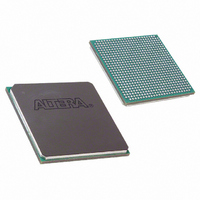
EP1SGX10DF672C5N Altera, EP1SGX10DF672C5N Datasheet - Page 7

EP1SGX10DF672C5N
Manufacturer Part Number
EP1SGX10DF672C5N
Description
IC STRATIX GX FPGA 10KLE 672FBGA
Manufacturer
Altera
Series
Stratix® GXr
Datasheet
1.EP1SGX10CF672C7N.pdf
(272 pages)
Specifications of EP1SGX10DF672C5N
Number Of Logic Elements/cells
10570
Number Of Labs/clbs
1057
Total Ram Bits
920448
Number Of I /o
362
Voltage - Supply
1.425 V ~ 1.575 V
Mounting Type
Surface Mount
Operating Temperature
0°C ~ 85°C
Package / Case
672-FBGA
Lead Free Status / RoHS Status
Lead free / RoHS Compliant
Number Of Gates
-
Available stocks
Company
Part Number
Manufacturer
Quantity
Price
- Current page: 7 of 272
- Download datasheet (3Mb)
Figure 1–1. Stratix GX I/O Blocks
Notes to
(1)
(2)
(3)
(4)
(5)
FPGA Functional
Description
Altera Corporation
February 2005
PLL8
PLL7
PLL1
PLL2
Figure 1–1
Banks 9 through 12 are enhanced PLL external clock output banks.
If the high-speed differential I/O pins are not used for high-speed differential signaling, they can support all of the
I/O standards except HSTL class I and II, GTL, SSTL-18 Class II, PCI, PCI-X, and AGP 1×/2×.
For guidelines for placing single-ended I/O pads next to differential I/O pads, see the Selectable I/O Standards in
Stratix & Stratix GX Devices chapter of the Stratix GX Device Handbook, Volume 2.
These I/O banks in Stratix GX devices also support the LVDS, LVPECL, and 3.3-V PCML I/O standards on
reference clocks and receiver input pins (AC coupled).
VREF1B3 VREF2B3 VREF3B3 VREF4B3 VREF5B3
VREF5B8 VREF4B8 VREF3B8 VREF2B8 VREF1B8
DQST9
DQSB9
(4)
(4)
Figure
DQST8
DQSB8
and HyperTransport I/O Block
LVDS, LVPECL, 3.3-V PCML,
and HyperTransport I/O Block
and Regular I/O Pins
LVDS, LVPECL, 3.3-V PCML,
is a top view of the Stratix GX silicon die.
1–1:
and Regular I/O Pins
DQST7
DQSB7
Bank 8
Bank 3
I/O Banks 1 and 2 Support All
Single-Ended I/O Standards Except
Differential HSTL Output Clocks,
Differential SSTL-2 Output Clocks,
HSTL Class II, GTL, SSTL-18 Class II,
PCI, PCI-X, and AGP 1 × /2 ×
DQSB6
DQST6
(3)
Stratix GX devices contain a two-dimensional row- and column-based
architecture to implement custom logic. A series of column and row
interconnects of varying length and speed provide signal interconnects
between logic array blocks (LABs), memory block structures, and DSP
blocks.
(3)
DQSB5
DQST5
Note (1)
I/O Banks 3, 4, 9 & 10 Support
All Single-Ended I/O Standards
I/O Banks 7, 8, 11 & 12 Support
All Single-Ended I/O Standards
11
9
PLL5
PLL6
10
12
PLL11
PLL12
VREF1B4 VREF2B4 VREF3B4 VREF4B4 VREF5B4
VREF5B7 VREF4B7 VREF3B7 VREF2B7 VREF1B7
DQST4
DQSB4
Introduction to the Stratix GX Device Data Sheet
(2)
1.5-V PCML
(2)
DQST3
DQSB3
(5)
Stratix GX Device Handbook, Volume 1
DQSB2
DQST2
Bank 7
Bank 4
DQST1
DQSB1
DQST0
DQSB0
I/O Bank 13
I/O Bank 14
I/O Bank 17
I/O Bank 16
I/O Bank 15
1–5
(5)
(5)
(5)
(5)
(5)
Related parts for EP1SGX10DF672C5N
Image
Part Number
Description
Manufacturer
Datasheet
Request
R

Part Number:
Description:
CYCLONE II STARTER KIT EP2C20N
Manufacturer:
Altera
Datasheet:

Part Number:
Description:
CPLD, EP610 Family, ECMOS Process, 300 Gates, 16 Macro Cells, 16 Reg., 16 User I/Os, 5V Supply, 35 Speed Grade, 24DIP
Manufacturer:
Altera Corporation
Datasheet:

Part Number:
Description:
CPLD, EP610 Family, ECMOS Process, 300 Gates, 16 Macro Cells, 16 Reg., 16 User I/Os, 5V Supply, 15 Speed Grade, 24DIP
Manufacturer:
Altera Corporation
Datasheet:

Part Number:
Description:
Manufacturer:
Altera Corporation
Datasheet:

Part Number:
Description:
CPLD, EP610 Family, ECMOS Process, 300 Gates, 16 Macro Cells, 16 Reg., 16 User I/Os, 5V Supply, 30 Speed Grade, 24DIP
Manufacturer:
Altera Corporation
Datasheet:

Part Number:
Description:
High-performance, low-power erasable programmable logic devices with 8 macrocells, 10ns
Manufacturer:
Altera Corporation
Datasheet:

Part Number:
Description:
High-performance, low-power erasable programmable logic devices with 8 macrocells, 7ns
Manufacturer:
Altera Corporation
Datasheet:

Part Number:
Description:
Classic EPLD
Manufacturer:
Altera Corporation
Datasheet:

Part Number:
Description:
High-performance, low-power erasable programmable logic devices with 8 macrocells, 10ns
Manufacturer:
Altera Corporation
Datasheet:

Part Number:
Description:
Manufacturer:
Altera Corporation
Datasheet:

Part Number:
Description:
Manufacturer:
Altera Corporation
Datasheet:

Part Number:
Description:
Manufacturer:
Altera Corporation
Datasheet:

Part Number:
Description:
CPLD, EP610 Family, ECMOS Process, 300 Gates, 16 Macro Cells, 16 Reg., 16 User I/Os, 5V Supply, 25 Speed Grade, 24DIP
Manufacturer:
Altera Corporation
Datasheet:


