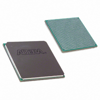
EP1SGX10DF672C5N Altera, EP1SGX10DF672C5N Datasheet - Page 62

EP1SGX10DF672C5N
Manufacturer Part Number
EP1SGX10DF672C5N
Description
IC STRATIX GX FPGA 10KLE 672FBGA
Manufacturer
Altera
Series
Stratix® GXr
Datasheet
1.EP1SGX10CF672C7N.pdf
(272 pages)
Specifications of EP1SGX10DF672C5N
Number Of Logic Elements/cells
10570
Number Of Labs/clbs
1057
Total Ram Bits
920448
Number Of I /o
362
Voltage - Supply
1.425 V ~ 1.575 V
Mounting Type
Surface Mount
Operating Temperature
0°C ~ 85°C
Package / Case
672-FBGA
Lead Free Status / RoHS Status
Lead free / RoHS Compliant
Number Of Gates
-
Available stocks
Company
Part Number
Manufacturer
Quantity
Price
- Current page: 62 of 272
- Download datasheet (3Mb)
Introduction
3–12
Stratix GX Device Handbook, Volume 1
The actual lock time for different data patterns varies depending on the
data’s transition density (how often the data switches between 1 and 0)
and jitter characteristic. The DPA circuitry is designed to lock onto any
data pattern with sufficient transition density, so the circuitry works with
current and future protocols. Experiments and simulations show that the
DPA circuitry locks when the data patterns listed in
repeated for the specified number of times. There are other suitable
patterns not shown in
may vary. The circuit can adjust for any phase variation that may occur
during operation.
Phase Synchronizer
Each receiver has its own phase synchronizer. The receiver phase
synchronizer aligns the phase of the parallel data from all the receivers to
one global clock. The synchronizers in each channel consist of a 4-bit deep
and J-bit wide FIFO buffer. The parallel clock writes to the FIFO buffer
and the global clock (GCLK) reads from the FIFO buffer. The global and
parallel clock inputs into the synchronizers must have identical
frequencies and differ only in phase. The FIFO buffer never becomes full
or empty (because the source and receive signals are frequency locked)
when operating within the DPA specifications, and the operation does
not require an empty/full flag or read/write enable signals.
Receiver Data Realignment In DPA Mode
While DPA operation aligns the incoming clock phase to the incoming
data phase, it does not guarantee the parallelization boundary or byte
boundary. When the dynamic phase aligner realigns the data bits, the bits
may be shifted out of byte alignment, as shown in
SPI-4, NPSI
RapidIO
Other designs
SFI-4, XSBI
Table 3–4. Training Patterns for Different Protocols
Protocols
Ten 0’s, ten 1’s
(
Four 0’s, four 1’s (
two 0’s, one 1, four 0’s (
Eight alternating 1’s and 0’s (
01010101
Not specified
00000000001111111111
Table 3–4
)
Training Pattern
and/or pattern lengths, but the lock time
00001111
10010000
10101010
) or one 1,
)
)
Figure
Table 3–4
Altera Corporation
or
3–10.
August 2005
Repetitions
Number of
are
256
Related parts for EP1SGX10DF672C5N
Image
Part Number
Description
Manufacturer
Datasheet
Request
R

Part Number:
Description:
CYCLONE II STARTER KIT EP2C20N
Manufacturer:
Altera
Datasheet:

Part Number:
Description:
CPLD, EP610 Family, ECMOS Process, 300 Gates, 16 Macro Cells, 16 Reg., 16 User I/Os, 5V Supply, 35 Speed Grade, 24DIP
Manufacturer:
Altera Corporation
Datasheet:

Part Number:
Description:
CPLD, EP610 Family, ECMOS Process, 300 Gates, 16 Macro Cells, 16 Reg., 16 User I/Os, 5V Supply, 15 Speed Grade, 24DIP
Manufacturer:
Altera Corporation
Datasheet:

Part Number:
Description:
Manufacturer:
Altera Corporation
Datasheet:

Part Number:
Description:
CPLD, EP610 Family, ECMOS Process, 300 Gates, 16 Macro Cells, 16 Reg., 16 User I/Os, 5V Supply, 30 Speed Grade, 24DIP
Manufacturer:
Altera Corporation
Datasheet:

Part Number:
Description:
High-performance, low-power erasable programmable logic devices with 8 macrocells, 10ns
Manufacturer:
Altera Corporation
Datasheet:

Part Number:
Description:
High-performance, low-power erasable programmable logic devices with 8 macrocells, 7ns
Manufacturer:
Altera Corporation
Datasheet:

Part Number:
Description:
Classic EPLD
Manufacturer:
Altera Corporation
Datasheet:

Part Number:
Description:
High-performance, low-power erasable programmable logic devices with 8 macrocells, 10ns
Manufacturer:
Altera Corporation
Datasheet:

Part Number:
Description:
Manufacturer:
Altera Corporation
Datasheet:

Part Number:
Description:
Manufacturer:
Altera Corporation
Datasheet:

Part Number:
Description:
Manufacturer:
Altera Corporation
Datasheet:

Part Number:
Description:
CPLD, EP610 Family, ECMOS Process, 300 Gates, 16 Macro Cells, 16 Reg., 16 User I/Os, 5V Supply, 25 Speed Grade, 24DIP
Manufacturer:
Altera Corporation
Datasheet:


