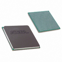
EP1SGX10DF672C5N Altera, EP1SGX10DF672C5N Datasheet - Page 74

EP1SGX10DF672C5N
Manufacturer Part Number
EP1SGX10DF672C5N
Description
IC STRATIX GX FPGA 10KLE 672FBGA
Manufacturer
Altera
Series
Stratix® GXr
Datasheet
1.EP1SGX10CF672C7N.pdf
(272 pages)
Specifications of EP1SGX10DF672C5N
Number Of Logic Elements/cells
10570
Number Of Labs/clbs
1057
Total Ram Bits
920448
Number Of I /o
362
Voltage - Supply
1.425 V ~ 1.575 V
Mounting Type
Surface Mount
Operating Temperature
0°C ~ 85°C
Package / Case
672-FBGA
Lead Free Status / RoHS Status
Lead free / RoHS Compliant
Number Of Gates
-
Available stocks
Company
Part Number
Manufacturer
Quantity
Price
- Current page: 74 of 272
- Download datasheet (3Mb)
Logic Elements
Figure 4–6. LE in Dynamic Arithmetic Mode
Note to
(1)
4–8
Stratix GX Device Handbook, Volume 1
The addnsub signal is tied to the carry input for the first LE of a carry chain only.
Figure
LAB Carry-In
Carry-In0
Carry-In1
data1
data2
data3
(LAB Wide)
addnsub
4–6:
(1)
Carry-Select Chain
The carry-select chain provides a very fast carry-select function between
LEs in arithmetic mode. The carry-select chain uses the redundant carry
calculation to increase the speed of carry functions. The LE is configured
to calculate outputs for a possible carry-in of 1 and carry-in of 0 in
parallel. The carry-in0 and carry-in1 signals from a lower-order bit
feed forward into the higher-order bit via the parallel carry chain and
feed into both the LUT and the next portion of the carry chain. Carry-
select chains can begin in any LE within an LAB.
The speed advantage of the carry-select chain is in the parallel
pre-computation of carry chains. Because the LAB carry-in selects the
precomputed carry chain, not every LE is in the critical path. Only the
propagation delay between LAB carry-in generation (LE 5 and LE 10) are
now part of the critical path. This feature allows the Stratix GX
architecture to implement high-speed counters, adders, multipliers,
parity functions, and comparators of arbitrary width.
Figure 4–7
adder. One portion of the LUT generates the sum of two bits using the
input signals and the appropriate carry-in bit; the sum is routed to the
output of the LE. The register can be bypassed for simple adders or used
Carry-Out0
LUT
LUT
LUT
LUT
Carry-Out1
shows the carry-select circuitry in an LAB for a 10-bit full
Register chain
connection
clock (LAB Wide)
(LAB Wide)
ena (LAB Wide)
aclr (LAB Wide)
sload
(LAB Wide)
Register Feedback
sclear
(LAB Wide)
ADATA
ENA
D
ALD/PRE
aload
CLRN
Q
Altera Corporation
Row, column, and
direct link routing
Row, column, and
direct link routing
Local routing
LUT chain
connection
Register
chain output
February 2005
Related parts for EP1SGX10DF672C5N
Image
Part Number
Description
Manufacturer
Datasheet
Request
R

Part Number:
Description:
CYCLONE II STARTER KIT EP2C20N
Manufacturer:
Altera
Datasheet:

Part Number:
Description:
CPLD, EP610 Family, ECMOS Process, 300 Gates, 16 Macro Cells, 16 Reg., 16 User I/Os, 5V Supply, 35 Speed Grade, 24DIP
Manufacturer:
Altera Corporation
Datasheet:

Part Number:
Description:
CPLD, EP610 Family, ECMOS Process, 300 Gates, 16 Macro Cells, 16 Reg., 16 User I/Os, 5V Supply, 15 Speed Grade, 24DIP
Manufacturer:
Altera Corporation
Datasheet:

Part Number:
Description:
Manufacturer:
Altera Corporation
Datasheet:

Part Number:
Description:
CPLD, EP610 Family, ECMOS Process, 300 Gates, 16 Macro Cells, 16 Reg., 16 User I/Os, 5V Supply, 30 Speed Grade, 24DIP
Manufacturer:
Altera Corporation
Datasheet:

Part Number:
Description:
High-performance, low-power erasable programmable logic devices with 8 macrocells, 10ns
Manufacturer:
Altera Corporation
Datasheet:

Part Number:
Description:
High-performance, low-power erasable programmable logic devices with 8 macrocells, 7ns
Manufacturer:
Altera Corporation
Datasheet:

Part Number:
Description:
Classic EPLD
Manufacturer:
Altera Corporation
Datasheet:

Part Number:
Description:
High-performance, low-power erasable programmable logic devices with 8 macrocells, 10ns
Manufacturer:
Altera Corporation
Datasheet:

Part Number:
Description:
Manufacturer:
Altera Corporation
Datasheet:

Part Number:
Description:
Manufacturer:
Altera Corporation
Datasheet:

Part Number:
Description:
Manufacturer:
Altera Corporation
Datasheet:

Part Number:
Description:
CPLD, EP610 Family, ECMOS Process, 300 Gates, 16 Macro Cells, 16 Reg., 16 User I/Os, 5V Supply, 25 Speed Grade, 24DIP
Manufacturer:
Altera Corporation
Datasheet:


