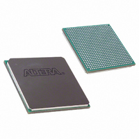
EP1SGX10DF672C5N Altera, EP1SGX10DF672C5N Datasheet - Page 175

EP1SGX10DF672C5N
Manufacturer Part Number
EP1SGX10DF672C5N
Description
IC STRATIX GX FPGA 10KLE 672FBGA
Manufacturer
Altera
Series
Stratix® GXr
Datasheet
1.EP1SGX10CF672C7N.pdf
(272 pages)
Specifications of EP1SGX10DF672C5N
Number Of Logic Elements/cells
10570
Number Of Labs/clbs
1057
Total Ram Bits
920448
Number Of I /o
362
Voltage - Supply
1.425 V ~ 1.575 V
Mounting Type
Surface Mount
Operating Temperature
0°C ~ 85°C
Package / Case
672-FBGA
Lead Free Status / RoHS Status
Lead free / RoHS Compliant
Number Of Gates
-
Available stocks
Company
Part Number
Manufacturer
Quantity
Price
- Current page: 175 of 272
- Download datasheet (3Mb)
Altera Corporation
February 2005
Notes to
(1)
(2)
(3)
EP1SGX10
EP1SGX25
EP1SGX40
Table 4–23. DQS & DQ Bus Mode Support
Device
See the Selectable I/O Standards in Stratix & Stratix GX Devices chapter of the Stratix GX Device Handbook,
Volume 2 for V
These packages have six groups in I/O banks 3 and 4 and six groups in I/O banks 7 and 8.
These packages have eight groups in I/O banks 3 and 4 and eight groups in I/O banks 7 and 8.
Table
672-pin FineLine BGA
672-pin FineLine BGA
1,020-pin FineLine BGA
1,020-pin FineLine BGA
4–23:
REF
guidelines.
Package
Table 4–23
per device.
A compensated delay element on each DQS pin automatically aligns
input DQS synchronization signals with the data window of their
corresponding DQ data signals. The DQS signals drive a local DQS bus in
the top and bottom I/O banks. This DQS bus is an additional resource to
the I/O clocks and clocks DQ input registers with the DQS signal.
Two separate single phase-shifting reference circuits are located on the
top and bottom of the Stratix GX device. Each circuit is driven by a system
reference clock through the CLK pins that is the same frequency as the
DQS signal. Clock pins CLK[15..12]p feed the phase-shift circuitry on
the top of the device and clock pins CLK[7..4]p feed the phase-shift
circuitry on the bottom of the device. The phase-shifting reference circuit
on the top of the device controls the compensated delay elements for all
10 DQS pins located at the top of the device. The phase-shifting reference
circuit on the bottom of the device controls the compensated delay
elements for all 10 DQS pins located on the bottom of the device. All
10 delay elements (DQS signals) on either the top or bottom of the device
shift by the same degree amount. For example, all 10 DQS pins on the top
of the device can be shifted by 90° and all 10 DQS pins on the bottom of
the device can be shifted by 72°. The reference circuits require a maximum
of 256 system reference clock cycles to set the correct phase on the DQS
delay elements.
control of each DQS delay shift on the top of the device. This same circuit
is duplicated on the bottom of the device.
shows the number of DQ and DQS buses that are supported
Figure 4–68
Note (1)
Number of ×8
Groups
12
16
20
20
(2)
(3)
illustrates the phase-shift reference circuit
Number of ×16
Stratix GX Device Handbook, Volume 1
Groups
0
8
8
8
Stratix GX Architecture
Number of ×32
Groups
0
4
4
4
4–109
Related parts for EP1SGX10DF672C5N
Image
Part Number
Description
Manufacturer
Datasheet
Request
R

Part Number:
Description:
CYCLONE II STARTER KIT EP2C20N
Manufacturer:
Altera
Datasheet:

Part Number:
Description:
CPLD, EP610 Family, ECMOS Process, 300 Gates, 16 Macro Cells, 16 Reg., 16 User I/Os, 5V Supply, 35 Speed Grade, 24DIP
Manufacturer:
Altera Corporation
Datasheet:

Part Number:
Description:
CPLD, EP610 Family, ECMOS Process, 300 Gates, 16 Macro Cells, 16 Reg., 16 User I/Os, 5V Supply, 15 Speed Grade, 24DIP
Manufacturer:
Altera Corporation
Datasheet:

Part Number:
Description:
Manufacturer:
Altera Corporation
Datasheet:

Part Number:
Description:
CPLD, EP610 Family, ECMOS Process, 300 Gates, 16 Macro Cells, 16 Reg., 16 User I/Os, 5V Supply, 30 Speed Grade, 24DIP
Manufacturer:
Altera Corporation
Datasheet:

Part Number:
Description:
High-performance, low-power erasable programmable logic devices with 8 macrocells, 10ns
Manufacturer:
Altera Corporation
Datasheet:

Part Number:
Description:
High-performance, low-power erasable programmable logic devices with 8 macrocells, 7ns
Manufacturer:
Altera Corporation
Datasheet:

Part Number:
Description:
Classic EPLD
Manufacturer:
Altera Corporation
Datasheet:

Part Number:
Description:
High-performance, low-power erasable programmable logic devices with 8 macrocells, 10ns
Manufacturer:
Altera Corporation
Datasheet:

Part Number:
Description:
Manufacturer:
Altera Corporation
Datasheet:

Part Number:
Description:
Manufacturer:
Altera Corporation
Datasheet:

Part Number:
Description:
Manufacturer:
Altera Corporation
Datasheet:

Part Number:
Description:
CPLD, EP610 Family, ECMOS Process, 300 Gates, 16 Macro Cells, 16 Reg., 16 User I/Os, 5V Supply, 25 Speed Grade, 24DIP
Manufacturer:
Altera Corporation
Datasheet:


