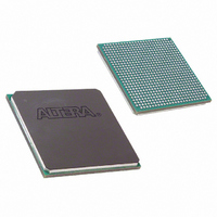
EP1SGX10DF672C5N Altera, EP1SGX10DF672C5N Datasheet - Page 215

EP1SGX10DF672C5N
Manufacturer Part Number
EP1SGX10DF672C5N
Description
IC STRATIX GX FPGA 10KLE 672FBGA
Manufacturer
Altera
Series
Stratix® GXr
Datasheet
1.EP1SGX10CF672C7N.pdf
(272 pages)
Specifications of EP1SGX10DF672C5N
Number Of Logic Elements/cells
10570
Number Of Labs/clbs
1057
Total Ram Bits
920448
Number Of I /o
362
Voltage - Supply
1.425 V ~ 1.575 V
Mounting Type
Surface Mount
Operating Temperature
0°C ~ 85°C
Package / Case
672-FBGA
Lead Free Status / RoHS Status
Lead free / RoHS Compliant
Number Of Gates
-
Available stocks
Company
Part Number
Manufacturer
Quantity
Price
- Current page: 215 of 272
- Download datasheet (3Mb)
Figure 6–2. Receiver Input Waveform Example with Values
Notes to
(1)
(2)
(3)
Figure 6–3. Transmitter Output Waveforms for Differential I/O Standards
Altera Corporation
June 2006
The values in this figure are for example only.
These values must meet the voltages specified in the section
If internal termination is used, the common mode is generated after the pins.
Figure
Single-Ended Waveform
Differential Waveform
Channel (p)
Channel (n)
Negative
Positive
6–2:
Ground
Single-Ended Waveform:
What is Applied
to the Pin (2)
Differential Waveform:
As Seen by the Buffer
or by Subtraction on an Oscilloscope
p - n = 0 V
V
CM
V
ID
V
ICM
Differential V
= 1.175 V (3)
V
ID
V
= 1 V
ID
ID
= 2 * V
(V ID (Differential) = 2 x V ID (single-ended))
V
ID
ID
= 1 V
(Single-Ended) = 2 V
“Operating Conditions” on page
Stratix GX Device Handbook, Volume 1
V
V
IH
ID
= 1.175 V + 0.5 V = 1.675 V
V
V
p − n = 0 V
IL
Positive Channel (p) = V
Negative Channel (n) = V
Ground
ID
= 1.175 V - 0.5 V = 0.675 V
= 1 V
DC & Switching Characteristics
6–1.
OH
OL
6–13
Related parts for EP1SGX10DF672C5N
Image
Part Number
Description
Manufacturer
Datasheet
Request
R

Part Number:
Description:
CYCLONE II STARTER KIT EP2C20N
Manufacturer:
Altera
Datasheet:

Part Number:
Description:
CPLD, EP610 Family, ECMOS Process, 300 Gates, 16 Macro Cells, 16 Reg., 16 User I/Os, 5V Supply, 35 Speed Grade, 24DIP
Manufacturer:
Altera Corporation
Datasheet:

Part Number:
Description:
CPLD, EP610 Family, ECMOS Process, 300 Gates, 16 Macro Cells, 16 Reg., 16 User I/Os, 5V Supply, 15 Speed Grade, 24DIP
Manufacturer:
Altera Corporation
Datasheet:

Part Number:
Description:
Manufacturer:
Altera Corporation
Datasheet:

Part Number:
Description:
CPLD, EP610 Family, ECMOS Process, 300 Gates, 16 Macro Cells, 16 Reg., 16 User I/Os, 5V Supply, 30 Speed Grade, 24DIP
Manufacturer:
Altera Corporation
Datasheet:

Part Number:
Description:
High-performance, low-power erasable programmable logic devices with 8 macrocells, 10ns
Manufacturer:
Altera Corporation
Datasheet:

Part Number:
Description:
High-performance, low-power erasable programmable logic devices with 8 macrocells, 7ns
Manufacturer:
Altera Corporation
Datasheet:

Part Number:
Description:
Classic EPLD
Manufacturer:
Altera Corporation
Datasheet:

Part Number:
Description:
High-performance, low-power erasable programmable logic devices with 8 macrocells, 10ns
Manufacturer:
Altera Corporation
Datasheet:

Part Number:
Description:
Manufacturer:
Altera Corporation
Datasheet:

Part Number:
Description:
Manufacturer:
Altera Corporation
Datasheet:

Part Number:
Description:
Manufacturer:
Altera Corporation
Datasheet:

Part Number:
Description:
CPLD, EP610 Family, ECMOS Process, 300 Gates, 16 Macro Cells, 16 Reg., 16 User I/Os, 5V Supply, 25 Speed Grade, 24DIP
Manufacturer:
Altera Corporation
Datasheet:


