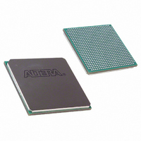
EP1SGX10DF672C5N Altera, EP1SGX10DF672C5N Datasheet - Page 212

EP1SGX10DF672C5N
Manufacturer Part Number
EP1SGX10DF672C5N
Description
IC STRATIX GX FPGA 10KLE 672FBGA
Manufacturer
Altera
Series
Stratix® GXr
Datasheet
1.EP1SGX10CF672C7N.pdf
(272 pages)
Specifications of EP1SGX10DF672C5N
Number Of Logic Elements/cells
10570
Number Of Labs/clbs
1057
Total Ram Bits
920448
Number Of I /o
362
Voltage - Supply
1.425 V ~ 1.575 V
Mounting Type
Surface Mount
Operating Temperature
0°C ~ 85°C
Package / Case
672-FBGA
Lead Free Status / RoHS Status
Lead free / RoHS Compliant
Number Of Gates
-
Available stocks
Company
Part Number
Manufacturer
Quantity
Price
- Current page: 212 of 272
- Download datasheet (3Mb)
Operating Conditions
6–10
Stratix GX Device Handbook, Volume 1
Notes to
(1)
(2)
(3)
(4)
(5)
(6)
(7)
(8)
(9)
(10) The numbers are for 3.125-Gbps data rate for –5 and –6 devices and 2.5 Gbps for –7 devices.
(11) Transmitter latency delay from parallel transceiver data to serial transceiver out data.
(12) The receiver operates with a BER of better than 10
Output return
loss
V
V
V
V
V
V
V
V
Description
Table 6–7. Stratix GX Transceiver Block AC Specification (Part 7 of 7)
Table 6–8. LVTTL Specifications
Table 6–9. LVCMOS Specifications
CCIO
I H
IL
OH
OL
CCIO
IH
IL
Symbol /
Symbol
Symbol
All numbers for the -6 and -7 speed grades are for both commercial and industrial unless specified otherwise in the
Conditions column. Speed grade -5 is available only for commercial specifications.
Not all V
jitter was added is 1,000 mV and the equalizer was set to the maximum condition of 111 (equalizer control setting
= 4 in the MegaWizard Plug-In Manager).
Number of parallel clocks.
Receive latency delay from serial receiver indata to parallel receiver data.
Per IEEE Standard 802.3ae @ 3.125 for –5 and –6.
The specification is for channel aligner tolerance.
UI = Unit Interval.
Run-length conditions are true for all data rates, but the average transition density must be enough to keep the
receiver phase aligned and the overall data must be DC balanced.
Not all combinations of V
template for 3.125 Gbps and in the PCI Exp transmitter eye mask for 2.5 Gbps.
Table
ID
Output supply voltage
High-level input voltage
Low-level input voltage
High-level output voltage
Low-level output voltage
6–7:
100 MHz to
2.5 GHz
and equalizer values will get the same results. The condition for the specification was that the V
Conditions
High-level input voltage
Low-level input voltage
Output supply voltage
Parameter
Parameter
OD
and pre-emphasis will get the same results.
Min
–10
Speed Grade
-5 Commercial
Typ
I
I
Max
OH
OL
-12
(1)
= 4 to 24 mA
= –4 to –24 mA
in the presence of an input signal as defined in the XAUI driver
Conditions
Conditions
Min
–10
-6 Commercial &
Industrial Speed
Typ
Grade
(1)
(1)
(1)
Max
Minimum
Minimum
–0.5
–0.5
3.0
1.7
2.4
3.0
1.7
Min
–10
-7 Commercial &
Industrial Speed
Maximum
Maximum
Grade
Typ
(1)
Altera Corporation
0.45
3.6
4.1
0.7
3.6
4.1
0.7
Max
June 2006
ID
Units
Units
before
V
V
V
V
V
V
V
V
Unit
dB
Related parts for EP1SGX10DF672C5N
Image
Part Number
Description
Manufacturer
Datasheet
Request
R

Part Number:
Description:
CYCLONE II STARTER KIT EP2C20N
Manufacturer:
Altera
Datasheet:

Part Number:
Description:
CPLD, EP610 Family, ECMOS Process, 300 Gates, 16 Macro Cells, 16 Reg., 16 User I/Os, 5V Supply, 35 Speed Grade, 24DIP
Manufacturer:
Altera Corporation
Datasheet:

Part Number:
Description:
CPLD, EP610 Family, ECMOS Process, 300 Gates, 16 Macro Cells, 16 Reg., 16 User I/Os, 5V Supply, 15 Speed Grade, 24DIP
Manufacturer:
Altera Corporation
Datasheet:

Part Number:
Description:
Manufacturer:
Altera Corporation
Datasheet:

Part Number:
Description:
CPLD, EP610 Family, ECMOS Process, 300 Gates, 16 Macro Cells, 16 Reg., 16 User I/Os, 5V Supply, 30 Speed Grade, 24DIP
Manufacturer:
Altera Corporation
Datasheet:

Part Number:
Description:
High-performance, low-power erasable programmable logic devices with 8 macrocells, 10ns
Manufacturer:
Altera Corporation
Datasheet:

Part Number:
Description:
High-performance, low-power erasable programmable logic devices with 8 macrocells, 7ns
Manufacturer:
Altera Corporation
Datasheet:

Part Number:
Description:
Classic EPLD
Manufacturer:
Altera Corporation
Datasheet:

Part Number:
Description:
High-performance, low-power erasable programmable logic devices with 8 macrocells, 10ns
Manufacturer:
Altera Corporation
Datasheet:

Part Number:
Description:
Manufacturer:
Altera Corporation
Datasheet:

Part Number:
Description:
Manufacturer:
Altera Corporation
Datasheet:

Part Number:
Description:
Manufacturer:
Altera Corporation
Datasheet:

Part Number:
Description:
CPLD, EP610 Family, ECMOS Process, 300 Gates, 16 Macro Cells, 16 Reg., 16 User I/Os, 5V Supply, 25 Speed Grade, 24DIP
Manufacturer:
Altera Corporation
Datasheet:


