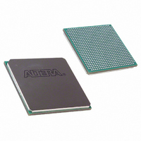
EP1SGX10DF672C5N Altera, EP1SGX10DF672C5N Datasheet - Page 187

EP1SGX10DF672C5N
Manufacturer Part Number
EP1SGX10DF672C5N
Description
IC STRATIX GX FPGA 10KLE 672FBGA
Manufacturer
Altera
Series
Stratix® GXr
Datasheet
1.EP1SGX10CF672C7N.pdf
(272 pages)
Specifications of EP1SGX10DF672C5N
Number Of Logic Elements/cells
10570
Number Of Labs/clbs
1057
Total Ram Bits
920448
Number Of I /o
362
Voltage - Supply
1.425 V ~ 1.575 V
Mounting Type
Surface Mount
Operating Temperature
0°C ~ 85°C
Package / Case
672-FBGA
Lead Free Status / RoHS Status
Lead free / RoHS Compliant
Number Of Gates
-
Available stocks
Company
Part Number
Manufacturer
Quantity
Price
- Current page: 187 of 272
- Download datasheet (3Mb)
Power
Sequencing &
Hot Socketing
Altera Corporation
February 2005
Notes to
(1)
(2)
(3)
(4)
(5)
(6)
1.5
1.8
2.5
3.3
Table 4–32. Stratix GX MultiVolt I/O Support
To drive inputs higher than V
inputs to the device, enable the PCI clamping diode to prevent V
The input pin current may be slightly higher than the typical value.
Although V
at a different level can still interface with the Stratix GX device if it has inputs that tolerate the V
Stratix GX devices can be 5.0-V tolerant with the use of an external resistor and the internal PCI clamp diode.
This is the external signal that is driving the Stratix GX device.
This represents the system voltage that Stratix GX supports when a VCCIO pin is connected to a specific voltage
level. For example, when VCCIO is 3.3 V and if the I/O standard is LVTTL/LVCMOS, the output high of the signal
coming out from Stratix GX is 3.3 V and is compatible with 3.3-V or 5.0-V systems.
V
CCIO
Table
(V)
4–32:
CCIO
specifies the voltage necessary for the Stratix GX device to drive out, a receiving device powered
v
1.5 V
v
(2)
2.5-V, or 3.3-V power supply, depending on the output requirements.
The output levels are compatible with systems of the same voltage as the
power supply (for example, when VCCIO pins are connected to a 1.5-V
power supply, the output levels are compatible with 1.5-V systems).
When VCCIO pins are connected to a 3.3-V power supply, the output high
is 3.3 V and is compatible with 3.3-V or 5.0-V systems.
Table 4–32
Because Stratix GX devices can be used in a mixed-voltage environment,
they have been designed specifically to tolerate any possible power-up
sequence. Therefore, the VCCIO and VCCINT power supplies may be
powered in any order.
Signals can be driven into Stratix GX devices before and during power up
without damaging the device. In addition, Stratix GX devices do not
drive out during power up. Once operating conditions are reached and
the device is configured, Stratix GX devices operate as specified by the
user. For more information, see the Selectable I/O Standards in Stratix &
Stratix GX Devices chapter of the Stratix GX Device Handbook, Volume 2.
1.8 V
v
v
CCIO
Input Signal
but less than 4.1 V, disable the PCI clamping diode. However, to drive 5.0-V
v
v
v
2.5 V
v
summarizes Stratix GX MultiVolt I/O support.
(2)
(2)
(2)
(5)
v
v
3.3 V
v
v
Note (1)
(2)
(2)
v
5.0 V
(4)
I
from rising above 4.0 V.
v
v
v
1.5 V
v
Stratix GX Device Handbook, Volume 1
(3)
(3)
(3)
v
v
1.8 V
v
Output Signal
(3)
(3)
v
2.5 V
Stratix GX Architecture
v
(3)
(6)
CCIO
3.3 V
v
value.
5.0 V
4–121
v
Related parts for EP1SGX10DF672C5N
Image
Part Number
Description
Manufacturer
Datasheet
Request
R

Part Number:
Description:
CYCLONE II STARTER KIT EP2C20N
Manufacturer:
Altera
Datasheet:

Part Number:
Description:
CPLD, EP610 Family, ECMOS Process, 300 Gates, 16 Macro Cells, 16 Reg., 16 User I/Os, 5V Supply, 35 Speed Grade, 24DIP
Manufacturer:
Altera Corporation
Datasheet:

Part Number:
Description:
CPLD, EP610 Family, ECMOS Process, 300 Gates, 16 Macro Cells, 16 Reg., 16 User I/Os, 5V Supply, 15 Speed Grade, 24DIP
Manufacturer:
Altera Corporation
Datasheet:

Part Number:
Description:
Manufacturer:
Altera Corporation
Datasheet:

Part Number:
Description:
CPLD, EP610 Family, ECMOS Process, 300 Gates, 16 Macro Cells, 16 Reg., 16 User I/Os, 5V Supply, 30 Speed Grade, 24DIP
Manufacturer:
Altera Corporation
Datasheet:

Part Number:
Description:
High-performance, low-power erasable programmable logic devices with 8 macrocells, 10ns
Manufacturer:
Altera Corporation
Datasheet:

Part Number:
Description:
High-performance, low-power erasable programmable logic devices with 8 macrocells, 7ns
Manufacturer:
Altera Corporation
Datasheet:

Part Number:
Description:
Classic EPLD
Manufacturer:
Altera Corporation
Datasheet:

Part Number:
Description:
High-performance, low-power erasable programmable logic devices with 8 macrocells, 10ns
Manufacturer:
Altera Corporation
Datasheet:

Part Number:
Description:
Manufacturer:
Altera Corporation
Datasheet:

Part Number:
Description:
Manufacturer:
Altera Corporation
Datasheet:

Part Number:
Description:
Manufacturer:
Altera Corporation
Datasheet:

Part Number:
Description:
CPLD, EP610 Family, ECMOS Process, 300 Gates, 16 Macro Cells, 16 Reg., 16 User I/Os, 5V Supply, 25 Speed Grade, 24DIP
Manufacturer:
Altera Corporation
Datasheet:


