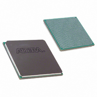
EP1SGX10DF672C5N Altera, EP1SGX10DF672C5N Datasheet - Page 8

EP1SGX10DF672C5N
Manufacturer Part Number
EP1SGX10DF672C5N
Description
IC STRATIX GX FPGA 10KLE 672FBGA
Manufacturer
Altera
Series
Stratix® GXr
Datasheet
1.EP1SGX10CF672C7N.pdf
(272 pages)
Specifications of EP1SGX10DF672C5N
Number Of Logic Elements/cells
10570
Number Of Labs/clbs
1057
Total Ram Bits
920448
Number Of I /o
362
Voltage - Supply
1.425 V ~ 1.575 V
Mounting Type
Surface Mount
Operating Temperature
0°C ~ 85°C
Package / Case
672-FBGA
Lead Free Status / RoHS Status
Lead free / RoHS Compliant
Number Of Gates
-
Available stocks
Company
Part Number
Manufacturer
Quantity
Price
- Current page: 8 of 272
- Download datasheet (3Mb)
FPGA Functional Description
1–6
Stratix GX Device Handbook, Volume 1
The logic array consists of LABs, with 10 logic elements (LEs) in each
LAB. An LE is a small unit of logic providing efficient implementation of
user logic functions. LABs are grouped into rows and columns across the
device.
M512 RAM blocks are simple dual-port memory blocks with 512 bits plus
parity (576 bits). These blocks provide dedicated simple dual-port or
single-port memory up to 18-bits wide at up to 318 MHz. M512 blocks are
grouped into columns across the device in between certain LABs.
M4K RAM blocks are true dual-port memory blocks with 4K bits plus
parity (4,608 bits). These blocks provide dedicated true dual-port, simple
dual-port, or single-port memory up to 36-bits wide at up to 291 MHz.
These blocks are grouped into columns across the device in between
certain LABs.
M-RAM blocks are true dual-port memory blocks with 512K bits plus
parity (589,824 bits). These blocks provide dedicated true dual-port,
simple dual-port, or single-port memory up to 144-bits wide at up to
269 MHz. Several M-RAM blocks are located individually or in pairs
within the device’s logic array.
Digital signal processing (DSP) blocks can implement up to either eight
full-precision 9 × 9-bit multipliers, four full-precision 18 × 18-bit
multipliers, or one full-precision 36 × 36-bit multiplier with add or
subtract features. These blocks also contain 18-bit input shift registers for
digital signal processing applications, including FIR and infinite impulse
response (IIR) filters. DSP blocks are grouped into two columns in each
device.
Each Stratix GX device I/O pin is fed by an I/O element (IOE) located at
the end of LAB rows and columns around the periphery of the device.
I/O pins support numerous single-ended and differential I/O standards.
Each IOE contains a bidirectional I/O buffer and six registers for
registering input, output, and output-enable signals. When used with
dedicated clocks, these registers provide exceptional performance and
interface support with external memory devices such as DDR SDRAM,
FCRAM, ZBT, and QDR SRAM devices.
High-speed serial interface channels support transfers at up to 840 Mbps
using LVDS, LVPECL, 3.3-V PCML, or HyperTransport technology I/O
standards.
Figure 1–2
shows an overview of the Stratix GX device.
Altera Corporation
February 2005
Related parts for EP1SGX10DF672C5N
Image
Part Number
Description
Manufacturer
Datasheet
Request
R

Part Number:
Description:
CYCLONE II STARTER KIT EP2C20N
Manufacturer:
Altera
Datasheet:

Part Number:
Description:
CPLD, EP610 Family, ECMOS Process, 300 Gates, 16 Macro Cells, 16 Reg., 16 User I/Os, 5V Supply, 35 Speed Grade, 24DIP
Manufacturer:
Altera Corporation
Datasheet:

Part Number:
Description:
CPLD, EP610 Family, ECMOS Process, 300 Gates, 16 Macro Cells, 16 Reg., 16 User I/Os, 5V Supply, 15 Speed Grade, 24DIP
Manufacturer:
Altera Corporation
Datasheet:

Part Number:
Description:
Manufacturer:
Altera Corporation
Datasheet:

Part Number:
Description:
CPLD, EP610 Family, ECMOS Process, 300 Gates, 16 Macro Cells, 16 Reg., 16 User I/Os, 5V Supply, 30 Speed Grade, 24DIP
Manufacturer:
Altera Corporation
Datasheet:

Part Number:
Description:
High-performance, low-power erasable programmable logic devices with 8 macrocells, 10ns
Manufacturer:
Altera Corporation
Datasheet:

Part Number:
Description:
High-performance, low-power erasable programmable logic devices with 8 macrocells, 7ns
Manufacturer:
Altera Corporation
Datasheet:

Part Number:
Description:
Classic EPLD
Manufacturer:
Altera Corporation
Datasheet:

Part Number:
Description:
High-performance, low-power erasable programmable logic devices with 8 macrocells, 10ns
Manufacturer:
Altera Corporation
Datasheet:

Part Number:
Description:
Manufacturer:
Altera Corporation
Datasheet:

Part Number:
Description:
Manufacturer:
Altera Corporation
Datasheet:

Part Number:
Description:
Manufacturer:
Altera Corporation
Datasheet:

Part Number:
Description:
CPLD, EP610 Family, ECMOS Process, 300 Gates, 16 Macro Cells, 16 Reg., 16 User I/Os, 5V Supply, 25 Speed Grade, 24DIP
Manufacturer:
Altera Corporation
Datasheet:


