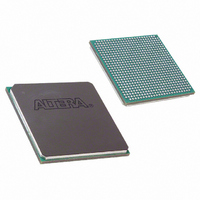
EP1SGX10DF672C5N Altera, EP1SGX10DF672C5N Datasheet - Page 54

EP1SGX10DF672C5N
Manufacturer Part Number
EP1SGX10DF672C5N
Description
IC STRATIX GX FPGA 10KLE 672FBGA
Manufacturer
Altera
Series
Stratix® GXr
Datasheet
1.EP1SGX10CF672C7N.pdf
(272 pages)
Specifications of EP1SGX10DF672C5N
Number Of Logic Elements/cells
10570
Number Of Labs/clbs
1057
Total Ram Bits
920448
Number Of I /o
362
Voltage - Supply
1.425 V ~ 1.575 V
Mounting Type
Surface Mount
Operating Temperature
0°C ~ 85°C
Package / Case
672-FBGA
Lead Free Status / RoHS Status
Lead free / RoHS Compliant
Number Of Gates
-
Available stocks
Company
Part Number
Manufacturer
Quantity
Price
- Current page: 54 of 272
- Download datasheet (3Mb)
Introduction
Figure 3–3. Stratix GX High-Speed Interface Serialized in
Figure 3–4. Transmitter Timing Diagram
3–4
Stratix GX Device Handbook, Volume 1
Internal ×10 clock
Internal ×1 clock
TXLOADEN
data input
Receiver
Stratix GX
Logic Array
n – 1
The logic array sends parallel data to the SERDES transmitter circuit
when the TXLOADEN signal is asserted. This signal is generated by the
high-speed counter circuitry of the logic array low-frequency clock’s
rising edge. The data is then transferred from the parallel register into the
serial shift register by the TXLOADEN signal on the third rising edge of the
high-frequency clock.
Figure 3–3
channel and
and clocks in Stratix GX devices in
multiplier and J is the data parallelization division factor.
n – 0
Transmitter Circuit
shows the block diagram of a single SERDES transmitter
PD9
PD8
PD7
PD6
PD5
PD4
PD3
PD2
PD0
PD1
9
Figure 3–4
Fast
PLL
8
Register
Parallel
× W
TXLOADEN
7
shows the timing relationship between the data
×
PD9
PD8
PD7
PD6
PD5
PD4
PD3
PD2
PD1
PD0
10 Mode
6
5
Register
×
Serial
10 mode. W is the low-frequency
4
3
2
Altera Corporation
1
TXOUT+
TXOUT−
August 2005
0
Related parts for EP1SGX10DF672C5N
Image
Part Number
Description
Manufacturer
Datasheet
Request
R

Part Number:
Description:
CYCLONE II STARTER KIT EP2C20N
Manufacturer:
Altera
Datasheet:

Part Number:
Description:
CPLD, EP610 Family, ECMOS Process, 300 Gates, 16 Macro Cells, 16 Reg., 16 User I/Os, 5V Supply, 35 Speed Grade, 24DIP
Manufacturer:
Altera Corporation
Datasheet:

Part Number:
Description:
CPLD, EP610 Family, ECMOS Process, 300 Gates, 16 Macro Cells, 16 Reg., 16 User I/Os, 5V Supply, 15 Speed Grade, 24DIP
Manufacturer:
Altera Corporation
Datasheet:

Part Number:
Description:
Manufacturer:
Altera Corporation
Datasheet:

Part Number:
Description:
CPLD, EP610 Family, ECMOS Process, 300 Gates, 16 Macro Cells, 16 Reg., 16 User I/Os, 5V Supply, 30 Speed Grade, 24DIP
Manufacturer:
Altera Corporation
Datasheet:

Part Number:
Description:
High-performance, low-power erasable programmable logic devices with 8 macrocells, 10ns
Manufacturer:
Altera Corporation
Datasheet:

Part Number:
Description:
High-performance, low-power erasable programmable logic devices with 8 macrocells, 7ns
Manufacturer:
Altera Corporation
Datasheet:

Part Number:
Description:
Classic EPLD
Manufacturer:
Altera Corporation
Datasheet:

Part Number:
Description:
High-performance, low-power erasable programmable logic devices with 8 macrocells, 10ns
Manufacturer:
Altera Corporation
Datasheet:

Part Number:
Description:
Manufacturer:
Altera Corporation
Datasheet:

Part Number:
Description:
Manufacturer:
Altera Corporation
Datasheet:

Part Number:
Description:
Manufacturer:
Altera Corporation
Datasheet:

Part Number:
Description:
CPLD, EP610 Family, ECMOS Process, 300 Gates, 16 Macro Cells, 16 Reg., 16 User I/Os, 5V Supply, 25 Speed Grade, 24DIP
Manufacturer:
Altera Corporation
Datasheet:


