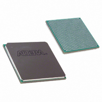
EP1SGX10DF672C5N Altera, EP1SGX10DF672C5N Datasheet - Page 17

EP1SGX10DF672C5N
Manufacturer Part Number
EP1SGX10DF672C5N
Description
IC STRATIX GX FPGA 10KLE 672FBGA
Manufacturer
Altera
Series
Stratix® GXr
Datasheet
1.EP1SGX10CF672C7N.pdf
(272 pages)
Specifications of EP1SGX10DF672C5N
Number Of Logic Elements/cells
10570
Number Of Labs/clbs
1057
Total Ram Bits
920448
Number Of I /o
362
Voltage - Supply
1.425 V ~ 1.575 V
Mounting Type
Surface Mount
Operating Temperature
0°C ~ 85°C
Package / Case
672-FBGA
Lead Free Status / RoHS Status
Lead free / RoHS Compliant
Number Of Gates
-
Available stocks
Company
Part Number
Manufacturer
Quantity
Price
- Current page: 17 of 272
- Download datasheet (3Mb)
Altera Corporation
June 2006
The transmitter PLL can support up to 3.1875 Mbps. The input clock
frequency for –5 and –6 speed grade devices is limited to 650 MHz if you
use the REFCLKB pin or to 325 MHz if you use the other clock routing
resources. For –7 speed grade devices, the maximum input clock
frequency is 312.5 MHz with the REFCLKB pin, and the maximum is
156.25 MHz for all other clock routing resources. An optional
PLL_LOCKED port is available to indicate whether the transmitter PLL is
locked to the reference clock. The transmitter PLL has a programmable
loop bandwidth that can be set to low or high. The loop bandwidth
parameter can be statically set in the Quartus II software.
Table 2–2
Transmitter Phase Compensation FIFO Buffer
The transmitter phase compensation FIFO buffer resides in the
transceiver block at the PLD boundary. This FIFO buffer compensates for
the phase differences between the transmitter reference clock (inclk)
and the PLD interface clock (tx_coreclk). The phase difference
between the two clocks must be less than 360° . The PLD interface clock
must also be frequency locked to the transmitter reference clock. The
phase compensation FIFO buffer is four words deep and cannot be
bypassed.
Byte Serializer
The byte serializer takes double-width words (16 or 20 bits) from the PLD
interface and converts them to a single width word (8 or 10 bits) for use
in the transceiver. The transmit data path after the byte serializer is single
width (8 or 10 bits). The byte serializer is bypassed when single width
mode (8 or 10 bits) is used at the PLD interface.
Note to
(1)
Input reference frequency range
Data rate support
Multiplication factor (W)
Bandwidth
Table 2–2. Transmitter PLL Specifications
Multiplication factors 2 and 5 can only be achieved with the use of the pre-divider
on the REFCLKB pin.
Table
lists the adjustable parameters in the transmitter PLL.
2–2:
Parameter
Stratix GX Device Handbook, Volume 1
25 MHz to 650 MHz
500 Mbps to 3.1875 Gbps
2, 4, 5, 8, 10, 16, or 20
Low, high
Specifications
Stratix GX Transceivers
(1)
2–7
Related parts for EP1SGX10DF672C5N
Image
Part Number
Description
Manufacturer
Datasheet
Request
R

Part Number:
Description:
CYCLONE II STARTER KIT EP2C20N
Manufacturer:
Altera
Datasheet:

Part Number:
Description:
CPLD, EP610 Family, ECMOS Process, 300 Gates, 16 Macro Cells, 16 Reg., 16 User I/Os, 5V Supply, 35 Speed Grade, 24DIP
Manufacturer:
Altera Corporation
Datasheet:

Part Number:
Description:
CPLD, EP610 Family, ECMOS Process, 300 Gates, 16 Macro Cells, 16 Reg., 16 User I/Os, 5V Supply, 15 Speed Grade, 24DIP
Manufacturer:
Altera Corporation
Datasheet:

Part Number:
Description:
Manufacturer:
Altera Corporation
Datasheet:

Part Number:
Description:
CPLD, EP610 Family, ECMOS Process, 300 Gates, 16 Macro Cells, 16 Reg., 16 User I/Os, 5V Supply, 30 Speed Grade, 24DIP
Manufacturer:
Altera Corporation
Datasheet:

Part Number:
Description:
High-performance, low-power erasable programmable logic devices with 8 macrocells, 10ns
Manufacturer:
Altera Corporation
Datasheet:

Part Number:
Description:
High-performance, low-power erasable programmable logic devices with 8 macrocells, 7ns
Manufacturer:
Altera Corporation
Datasheet:

Part Number:
Description:
Classic EPLD
Manufacturer:
Altera Corporation
Datasheet:

Part Number:
Description:
High-performance, low-power erasable programmable logic devices with 8 macrocells, 10ns
Manufacturer:
Altera Corporation
Datasheet:

Part Number:
Description:
Manufacturer:
Altera Corporation
Datasheet:

Part Number:
Description:
Manufacturer:
Altera Corporation
Datasheet:

Part Number:
Description:
Manufacturer:
Altera Corporation
Datasheet:

Part Number:
Description:
CPLD, EP610 Family, ECMOS Process, 300 Gates, 16 Macro Cells, 16 Reg., 16 User I/Os, 5V Supply, 25 Speed Grade, 24DIP
Manufacturer:
Altera Corporation
Datasheet:


