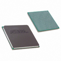
EP1SGX10DF672C5N Altera, EP1SGX10DF672C5N Datasheet - Page 193

EP1SGX10DF672C5N
Manufacturer Part Number
EP1SGX10DF672C5N
Description
IC STRATIX GX FPGA 10KLE 672FBGA
Manufacturer
Altera
Series
Stratix® GXr
Datasheet
1.EP1SGX10CF672C7N.pdf
(272 pages)
Specifications of EP1SGX10DF672C5N
Number Of Logic Elements/cells
10570
Number Of Labs/clbs
1057
Total Ram Bits
920448
Number Of I /o
362
Voltage - Supply
1.425 V ~ 1.575 V
Mounting Type
Surface Mount
Operating Temperature
0°C ~ 85°C
Package / Case
672-FBGA
Lead Free Status / RoHS Status
Lead free / RoHS Compliant
Number Of Gates
-
Available stocks
Company
Part Number
Manufacturer
Quantity
Price
- Current page: 193 of 272
- Download datasheet (3Mb)
SignalTap
Embedded Logic
Analyzer
Configuration
Altera Corporation
February 2005
SGX51005-1.0
Stratix
which monitors design operation over a period of time through the
IEEE Std. 1149.1 (JTAG) circuitry. You can analyze internal logic at speed
without bringing internal signals to the I/O pins. This feature is
particularly important for advanced packages, such as FineLine BGA
packages, because it can be difficult to add a connection to a pin during
the debugging process after a board is designed and manufactured.
The logic, circuitry, and interconnects in the Stratix GX architecture are
configured with CMOS SRAM elements. Stratix GX devices are
reconfigurable and are 100% tested prior to shipment. As a result, you do
not have to generate test vectors for fault coverage purposes, and can
instead focus on simulation and design verification. In addition, you do
not need to manage inventories of different ASIC designs. Stratix GX
devices can be configured on the board for the specific functionality
required.
Stratix GX devices are configured at system power-up with data stored in
an Altera serial configuration device or provided by a system controller.
Altera offers in-system programmability (ISP)-capable configuration
devices that configure Stratix GX devices via a serial data stream.
Stratix GX devices can be configured in under 100 ms using 8-bit parallel
data at 100 MHz. The Stratix GX device’s optimized interface allows
microprocessors to configure it serially or in parallel, and synchronously
or asynchronously. The interface also enables microprocessors to treat
Stratix GX devices as memory and configure them by writing to a virtual
memory location, making reconfiguration easy. After a Stratix GX device
has been configured, it can be reconfigured in-circuit by resetting the
device and loading new data. Real-time changes can be made during
system operation, enabling innovative reconfigurable computing
applications.
Operating Modes
The Stratix GX architecture uses SRAM configuration elements that
require configuration data to be loaded each time the circuit powers up.
The process of physically loading the SRAM data into the device is called
configuration. During initialization, which occurs immediately after
configuration, the device resets registers, enables I/O pins, and begins to
operate as a logic device. The I/O pins are tri-stated during power up,
®
GX devices feature the SignalTap
5. Configuration & Testing
®
embedded logic analyzer,
®
5–1
Related parts for EP1SGX10DF672C5N
Image
Part Number
Description
Manufacturer
Datasheet
Request
R

Part Number:
Description:
CYCLONE II STARTER KIT EP2C20N
Manufacturer:
Altera
Datasheet:

Part Number:
Description:
CPLD, EP610 Family, ECMOS Process, 300 Gates, 16 Macro Cells, 16 Reg., 16 User I/Os, 5V Supply, 35 Speed Grade, 24DIP
Manufacturer:
Altera Corporation
Datasheet:

Part Number:
Description:
CPLD, EP610 Family, ECMOS Process, 300 Gates, 16 Macro Cells, 16 Reg., 16 User I/Os, 5V Supply, 15 Speed Grade, 24DIP
Manufacturer:
Altera Corporation
Datasheet:

Part Number:
Description:
Manufacturer:
Altera Corporation
Datasheet:

Part Number:
Description:
CPLD, EP610 Family, ECMOS Process, 300 Gates, 16 Macro Cells, 16 Reg., 16 User I/Os, 5V Supply, 30 Speed Grade, 24DIP
Manufacturer:
Altera Corporation
Datasheet:

Part Number:
Description:
High-performance, low-power erasable programmable logic devices with 8 macrocells, 10ns
Manufacturer:
Altera Corporation
Datasheet:

Part Number:
Description:
High-performance, low-power erasable programmable logic devices with 8 macrocells, 7ns
Manufacturer:
Altera Corporation
Datasheet:

Part Number:
Description:
Classic EPLD
Manufacturer:
Altera Corporation
Datasheet:

Part Number:
Description:
High-performance, low-power erasable programmable logic devices with 8 macrocells, 10ns
Manufacturer:
Altera Corporation
Datasheet:

Part Number:
Description:
Manufacturer:
Altera Corporation
Datasheet:

Part Number:
Description:
Manufacturer:
Altera Corporation
Datasheet:

Part Number:
Description:
Manufacturer:
Altera Corporation
Datasheet:

Part Number:
Description:
CPLD, EP610 Family, ECMOS Process, 300 Gates, 16 Macro Cells, 16 Reg., 16 User I/Os, 5V Supply, 25 Speed Grade, 24DIP
Manufacturer:
Altera Corporation
Datasheet:


