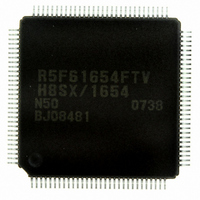
DF61654N50FTV Renesas Electronics America, DF61654N50FTV Datasheet - Page 193

DF61654N50FTV
Manufacturer Part Number
DF61654N50FTV
Description
IC H8SX/1654 MCU FLASH 120TQFP
Manufacturer
Renesas Electronics America
Series
H8® H8SX/1600r
Datasheet
1.DF61653N50FTV.pdf
(1020 pages)
Specifications of DF61654N50FTV
Core Processor
H8SX
Core Size
32-Bit
Speed
50MHz
Connectivity
I²C, IrDA, SCI, SmartCard, USB
Peripherals
DMA, PWM, WDT
Number Of I /o
75
Program Memory Size
512KB (512K x 8)
Program Memory Type
FLASH
Ram Size
40K x 8
Voltage - Supply (vcc/vdd)
3 V ~ 3.6 V
Data Converters
A/D 8x10b; D/A 2x8b
Oscillator Type
External
Operating Temperature
-20°C ~ 75°C
Package / Case
120-TQFP, 120-VQFP
For Use With
HS0005KCU11H - EMULATOR E10A-USB H8S(X),SH2(A)3DK1657 - DEV EVAL KIT FOR H8SX/1657
Lead Free Status / RoHS Status
Lead free / RoHS Compliant
Eeprom Size
-
Available stocks
Company
Part Number
Manufacturer
Quantity
Price
Company:
Part Number:
DF61654N50FTV
Manufacturer:
Renesas Electronics America
Quantity:
10 000
- Current page: 193 of 1020
- Download datasheet (6Mb)
Note: When external bus release is enabled or input by the WAIT pin is enabled, make sure to set
Bit
13, 12
11, 10
9
8
7
6
5 to 0
the ICR bit to 1. For details, see section 9, I/O Ports.
Bit Name
WDBE
WAITE
DKC
Initial
Value
All 0
All 0
0
0
0
0
All 0
R/W
R
R/W
R/W
R/W
R/W
R
R/W
Description
Reserved
These are read-only bits and cannot be modified.
Reserved
These bits are always read as 0. The write value should
always be 0.
Write Data Buffer Enable
The write data buffer function can be used for an
external write cycle and a DMAC single address
transfer cycle.
The changed setting may not affect an external access
immediately after the change.
0: Write data buffer function not used
1: Write data buffer function used
WAIT Pin Enable
Selects enabling/disabling of wait input by the WAIT
pin.
0: Wait input by WAIT pin disabled
1: Wait input by WAIT pin enabled
For details, see section 9, I/O Ports.
DACK Control
Selects the timing of DMAC transfer acknowledge
signal assertion.
0: DACK signal is asserted at the Bφ falling edge
1: DACK signal is asserted at the Bφ rising edge
Reserved
This bit is always read as 0. The write value should
always be 0.
Reserved
These are read-only bits and cannot be modified.
WAIT pin can be used as I/O port
Rev.1.00 Sep. 08, 2005 Page 143 of 966
Section 6 Bus Controller (BSC)
REJ09B0219-0100
Related parts for DF61654N50FTV
Image
Part Number
Description
Manufacturer
Datasheet
Request
R

Part Number:
Description:
KIT STARTER FOR M16C/29
Manufacturer:
Renesas Electronics America
Datasheet:

Part Number:
Description:
KIT STARTER FOR R8C/2D
Manufacturer:
Renesas Electronics America
Datasheet:

Part Number:
Description:
R0K33062P STARTER KIT
Manufacturer:
Renesas Electronics America
Datasheet:

Part Number:
Description:
KIT STARTER FOR R8C/23 E8A
Manufacturer:
Renesas Electronics America
Datasheet:

Part Number:
Description:
KIT STARTER FOR R8C/25
Manufacturer:
Renesas Electronics America
Datasheet:

Part Number:
Description:
KIT STARTER H8S2456 SHARPE DSPLY
Manufacturer:
Renesas Electronics America
Datasheet:

Part Number:
Description:
KIT STARTER FOR R8C38C
Manufacturer:
Renesas Electronics America
Datasheet:

Part Number:
Description:
KIT STARTER FOR R8C35C
Manufacturer:
Renesas Electronics America
Datasheet:

Part Number:
Description:
KIT STARTER FOR R8CL3AC+LCD APPS
Manufacturer:
Renesas Electronics America
Datasheet:

Part Number:
Description:
KIT STARTER FOR RX610
Manufacturer:
Renesas Electronics America
Datasheet:

Part Number:
Description:
KIT STARTER FOR R32C/118
Manufacturer:
Renesas Electronics America
Datasheet:

Part Number:
Description:
KIT DEV RSK-R8C/26-29
Manufacturer:
Renesas Electronics America
Datasheet:

Part Number:
Description:
KIT STARTER FOR SH7124
Manufacturer:
Renesas Electronics America
Datasheet:

Part Number:
Description:
KIT STARTER FOR H8SX/1622
Manufacturer:
Renesas Electronics America
Datasheet:

Part Number:
Description:
KIT DEV FOR SH7203
Manufacturer:
Renesas Electronics America
Datasheet:


