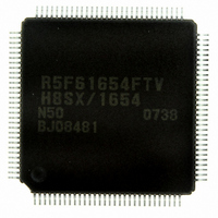
DF61654N50FTV Renesas Electronics America, DF61654N50FTV Datasheet - Page 355

DF61654N50FTV
Manufacturer Part Number
DF61654N50FTV
Description
IC H8SX/1654 MCU FLASH 120TQFP
Manufacturer
Renesas Electronics America
Series
H8® H8SX/1600r
Datasheet
1.DF61653N50FTV.pdf
(1020 pages)
Specifications of DF61654N50FTV
Core Processor
H8SX
Core Size
32-Bit
Speed
50MHz
Connectivity
I²C, IrDA, SCI, SmartCard, USB
Peripherals
DMA, PWM, WDT
Number Of I /o
75
Program Memory Size
512KB (512K x 8)
Program Memory Type
FLASH
Ram Size
40K x 8
Voltage - Supply (vcc/vdd)
3 V ~ 3.6 V
Data Converters
A/D 8x10b; D/A 2x8b
Oscillator Type
External
Operating Temperature
-20°C ~ 75°C
Package / Case
120-TQFP, 120-VQFP
For Use With
HS0005KCU11H - EMULATOR E10A-USB H8S(X),SH2(A)3DK1657 - DEV EVAL KIT FOR H8SX/1657
Lead Free Status / RoHS Status
Lead free / RoHS Compliant
Eeprom Size
-
Available stocks
Company
Part Number
Manufacturer
Quantity
Price
Company:
Part Number:
DF61654N50FTV
Manufacturer:
Renesas Electronics America
Quantity:
10 000
- Current page: 355 of 1020
- Download datasheet (6Mb)
7.9
1. DMAC Register Access During Operation
2. Settings of Module Stop Function
3. Activation by DREQ Falling Edge
4. Acceptation of Activation Source
Except for clearing the DTE bit in DMDR, the settings for channels being transferred
(including waiting state) must not be changed. The register settings must be changed during
the transfer prohibited state.
The DMAC operation can be enabled or disabled by the module stop control register. The
DMAC is enabled by the initial value.
Setting bit MSTPA13 in MSTPCRA stops the clock supplied to the DMAC and the DMAC
enters the module stop state. However, when a transfer for a channel is enabled or when an
interrupt is being requested, bit MSTPA13 cannot be set to 1. Clear the DTE bit to 0, clear the
DTIF or DTIE bit in DMDR to 0, and then set bit MSTPA13.
When the clock is stopped, the DMAC registers cannot be accessed. However, the following
register settings are valid in the module stop state. Disable them before entering the module
stop state, if necessary.
TENDE bit in DMDR is 1 (the TEND signal output enabled)
DACKE bit in DMDR is 1 (the DACK signal output enabled)
The DREQ falling edge detection is synchronized with the DMAC internal operation.
A. Activation request waiting state: Waiting for detecting the DREQ low level. A transition to
B. Transfer waiting state: Waiting for a DMAC transfer. A transition to 3. is made.
C. Transfer prohibited state: Waiting for detecting the DREQ high level. A transition to 1. is
After a DMAC transfer enabled, a transition to 1. is made. Therefore, the DREQ signal is
sampled by low level detection at the first activation after a DMAC transfer enabled.
At the beginning of an activation source reception, a low level is detected regardless of the
setting of DREQ falling edge or low level detection. Therefore, if the DREQ signal is driven
low before setting DMDR, the low level is received as a transfer request.
When the DMAC is activated, clear the DREQ signal of the previous transfer.
2. is made.
made.
Notes on Usage
Rev.1.00 Sep. 08, 2005 Page 305 of 966
Section 7 DMA Controller (DMAC)
REJ09B0219-0100
Related parts for DF61654N50FTV
Image
Part Number
Description
Manufacturer
Datasheet
Request
R

Part Number:
Description:
KIT STARTER FOR M16C/29
Manufacturer:
Renesas Electronics America
Datasheet:

Part Number:
Description:
KIT STARTER FOR R8C/2D
Manufacturer:
Renesas Electronics America
Datasheet:

Part Number:
Description:
R0K33062P STARTER KIT
Manufacturer:
Renesas Electronics America
Datasheet:

Part Number:
Description:
KIT STARTER FOR R8C/23 E8A
Manufacturer:
Renesas Electronics America
Datasheet:

Part Number:
Description:
KIT STARTER FOR R8C/25
Manufacturer:
Renesas Electronics America
Datasheet:

Part Number:
Description:
KIT STARTER H8S2456 SHARPE DSPLY
Manufacturer:
Renesas Electronics America
Datasheet:

Part Number:
Description:
KIT STARTER FOR R8C38C
Manufacturer:
Renesas Electronics America
Datasheet:

Part Number:
Description:
KIT STARTER FOR R8C35C
Manufacturer:
Renesas Electronics America
Datasheet:

Part Number:
Description:
KIT STARTER FOR R8CL3AC+LCD APPS
Manufacturer:
Renesas Electronics America
Datasheet:

Part Number:
Description:
KIT STARTER FOR RX610
Manufacturer:
Renesas Electronics America
Datasheet:

Part Number:
Description:
KIT STARTER FOR R32C/118
Manufacturer:
Renesas Electronics America
Datasheet:

Part Number:
Description:
KIT DEV RSK-R8C/26-29
Manufacturer:
Renesas Electronics America
Datasheet:

Part Number:
Description:
KIT STARTER FOR SH7124
Manufacturer:
Renesas Electronics America
Datasheet:

Part Number:
Description:
KIT STARTER FOR H8SX/1622
Manufacturer:
Renesas Electronics America
Datasheet:

Part Number:
Description:
KIT DEV FOR SH7203
Manufacturer:
Renesas Electronics America
Datasheet:


